


I've been in discussions with a component supplier who would like to sponsor a Design Challenge.
But its vision of the Design Challenge is a little different than how element14 typically administers a Design Challenge. I want to tell you the details below. I would really appreciate you voting in the polls and offering feedback on the challenge. Thanks.
Randall
-element14 Community Team
What is the Beat Our Board Design Challenge?
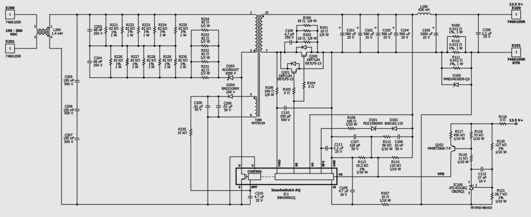
The goal of PI Beat Our Board Design Challenge is for the participants to design a board that improves or beats the sponsor's DER-953 board. Below, I've posted a short video and a schematic of this RDK, as well as the datasheet.
How Applicants are Selected as one of the Top 10
The Top 10 submissions get to advance to the next stage and will be given the DER-953Q plus a $250 shopping cart to buy materials – fulfilled by Farnell. The sponsor or its representatives will judge the finalists. They are awarding $5,000 to the grand prize winner and $2,500 to the 2nd place winner.
The enrollment period will last 6 weeks.
What they need to show to be one of the top 10
To be selected as one of the Top 10, the applicant needs to show the following:
• Topology / switch type
• Transformer size
• Preliminary schematic
The length of the challenge is about 6 months (ends June 2024).
Here are the criteria to win:
• Cannot use InnoSwitch
• Beat the efficiency – 10%, 25%, 50% and 100% no-load
• 40-500 V DC input
• Size/ volume of board must be same size or smaller
• Must meet thermals – 85 degrees Celsius – no heatsink
• No optocouplers
• Component count
• No-load consumption
• Automotive qualified components only
• Transformer exempt
• Up to and no more than a 6-layer PCB
• Specify PCB stack up weight per sq foot- 2oz 1oz 1oz 1oz 2: Maximum copper thickness on top and bottom layers
• Overload power current limit = 8.1 A
What do you think of this challenge? I invite you to offer your thoughts in the comments section below.
I also invite you to vote in the following polls:


