Designing and/or troubleshooting a system with, say, an MCU driving signals across transmission lines, can be an interesting exercise in patience and diligent sleuthing. Perhaps you're seeing an inordinate amount of bit errors at the receive end of I/O lines but having some difficulty nailing down the source. In many cases, the problem is ground bounce, an issue that can be tough to diagnose and cure. Let's begin an examination of the ground-bounce phenomenon by explaining how it arises and then outlining an approach for finding it.
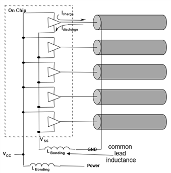
Figure 1: Shown are five I/O drivers within a package driving signal lines on a PC board
Figure 1 shows a few I/O drivers within an IC package (contained within dotted rectangle) feeding signals to some transmission lines on a PC board. The five I/O drivers shown share common Vcc and Vss rails on the die. As the drivers' signals go off chip, they'll traverse leads that reach from the die's bond pads to solder balls on the PC board and then to signal traces on the PCB. The common Vcc and Vss leads connect to solder balls on the PCB and connect to the PC board's ground and power planes.
As these I/O drivers push signals to various on-board destinations, suppose that the top four drivers in Figure 1 are switching, while we keep the bottom of the five drivers tied low, connecting its output to the Vss rail on the die. Say our four switching drivers make a transition from output high to output low, sending the charge stored on those transmission lines heading down the Vss rail into the board's return plane. That current will reach the ground plane, then travel underneath the signal lines. All of the switching current will have passed through the common lead inductance in the package.
When you have a transient current, a ΔI/Δt, traveling through the inductance of this common lead, a voltage results. Thus, the Vss rail on the IC package side of Lbonding in Figure 1 will have a higher potential than the Vss rail on the PCB ground-plane side of Lbonding. It's that connection between the package's solder ball to the PC board's ground plane that the current flows through to make its way under the signal line and continue its journey down the transmission line.
When that current gets to the solder ball, it encounters a low-impedance path in the ground plane. However, in leaving the package and passing through that solder ball, the current is constricted and forced through a narrow path in a common lead, which means there's a little more inductance in that path. So when we get the ΔI/Δt of the I/O drivers' switching, we'll have a voltage on one side relative to the other, and that voltage is connected to the fifth driver that's pegged low. We will see that voltage on the output of the low driver, and that little voltage bounce on the die side of Lbonding is going to propagate on the driver's associated transmission line and reach whatever that line is connected to as though it were a proper signal.
This quiet-low I/O driver is the key to diagnosing and evaluating ground bounce. By looking at this driver's output, we can deploy it as a sense line to tell us what the voltage is on the die's ground rail relative to the PC board's ground plane.
Figure 2: Shown are an I/O output signal (yellow) and a quiet-low I/O sense line (magenta) picking up ground bounce that results from the signal line's switching activity
Figure 2 shows a measured example of the voltage noise on a quiet-low line. The yellow trace is a switching I/O driver output while the magenta trace is the quiet low. When the driver goes high, we see a negative spike, and as it goes low, a positive spike, due to current traveling in opposite directions through Lbonding for these transitions. Those spikes in voltage on the quiet-low line are ground bounce.
You can see from Figure 2 why ground bounce can be so difficult to diagnose. When we have signal lines that are switching and we're monitoring the received signals on an oscilloscope, we might not be looking at our signals right on the edges. We might have our setup and hold times adjusted so that we're looking at the center of the pulse. If so, we probably will not detect the ground bounce.
If you're working with a synchronous bus, you might get away with engineering the timing such that you won't be all that sensitive to ground bounce. But if you're working with an asynchronous bus, as most of the common microcontroller buses such as I2C, SPI, or CANbus are, they are going to be highly susceptible to ground-bounce noise that can happen anywhere in a given clock cycle. The result is likely to be those bit errors mentioned above.
In upcoming posts, we'll look more closely at this quiet-low I/O driver approach to detecting ground bounce, as well as how to measure it effectively.


