element14 Community
element14 Community
    Register Log In
  • Site
  • Search
  • Log In Register
  • Members
    Members
    • Achievement Levels
    • Benefits of Membership
    • Feedback and Support
    • Members Area
    • Personal Blogs
    • What's New on element14
  • Learn
    Learn
    • eBooks
    • Learning Center
    • Learning Groups
    • STEM Academy
    • Webinars, Training and Events
  • Technologies
    Technologies
    • 3D Printing
    • Experts & Guidance
    • FPGA
    • Industrial Automation
    • Internet of Things
    • Power & Energy
    • Sensors
    • Technology Groups
  • Challenges & Projects
    Challenges & Projects
    • Arduino Projects
    • Design Challenges
    • element14 presents
    • Project14
    • Project Groups
    • Raspberry Pi Projects
  • Products
    Products
    • Arduino
    • Avnet Boards Community
    • Dev Tools
    • Manufacturers
    • Product Groups
    • Raspberry Pi
    • RoadTests & Reviews
  • Store
    Store
    • Visit Your Store
    • Or choose another store...
      • Europe
      •  Austria (German)
      •  Belgium (Dutch, French)
      •  Bulgaria (Bulgarian)
      •  Czech Republic (Czech)
      •  Denmark (Danish)
      •  Estonia (Estonian)
      •  Finland (Finnish)
      •  France (French)
      •  Germany (German)
      •  Hungary (Hungarian)
      •  Ireland
      •  Israel
      •  Italy (Italian)
      •  Latvia (Latvian)
      •  
      •  Lithuania (Lithuanian)
      •  Netherlands (Dutch)
      •  Norway (Norwegian)
      •  Poland (Polish)
      •  Portugal (Portuguese)
      •  Romania (Romanian)
      •  Russia (Russian)
      •  Slovakia (Slovak)
      •  Slovenia (Slovenian)
      •  Spain (Spanish)
      •  Sweden (Swedish)
      •  Switzerland(German, French)
      •  Turkey (Turkish)
      •  United Kingdom
      • Asia Pacific
      •  Australia
      •  China
      •  Hong Kong
      •  India
      •  Korea (Korean)
      •  Malaysia
      •  New Zealand
      •  Philippines
      •  Singapore
      •  Taiwan
      •  Thailand (Thai)
      • Americas
      •  Brazil (Portuguese)
      •  Canada
      •  Mexico (Spanish)
      •  United States
      Can't find the country/region you're looking for? Visit our export site or find a local distributor.
  • Translate
  • Profile
Personal Blogs
  • Members
  • More
Personal Blogs
Legacy Personal Blogs Booards and Boojums: Lattice XP2 Brevia2 Board: Part 2: Count Those LEDs!
  • Blog
  • Documents
  • Mentions
  • Sub-Groups
  • Tags
  • More
  • Cancel
  • New
Blog Post Actions
  • Subscribe by email
  • More
  • Cancel
  • Share
  • Subscribe by email
  • More
  • Cancel
Group Actions
  • Group RSS
  • More
  • Cancel
Engagement
  • Author Author: jc2048
  • Date Created: 27 Jan 2018 4:46 PM Date Created
  • Views 740 views
  • Likes 6 likes
  • Comments 1 comment
  • brevia2
  • fpgafeatured
  • fpga
  • vhdl
  • lattice
Related
Recommended

Booards and Boojums: Lattice XP2 Brevia2 Board: Part 2: Count Those LEDs!

jc2048
jc2048
27 Jan 2018

It seems 2018 is going to be the 'Year of the FPGA' here on element14 ('Forward Heroic Engineers of the World to a Flip-Flop Rich Future'), so I thought I'd join in, buy a small development board and do a simple project or two. The board I'm working with here is the Brevia2 board from Lattice[2].


Part 1 covered unpacking the board, connecting it to the computer and checking that it worked:


Booards and Boojums: Lattice XP2 Brevia2 Board: Part 1


In this part I'm going to try doing a very simple design in VHDL using the development tools (Diamond 3.10). Nothing too complicated - I'm just going to count in binary on the row of LEDs in the bottom corner. This will allow me to run through the design flow and see how similar the process is to what I've used before (Xilinx WebPack). Just for fun I'm going to see how far I can get without looking at the help files and other documentation.


Here's how the IDE looks at first start-up.


image


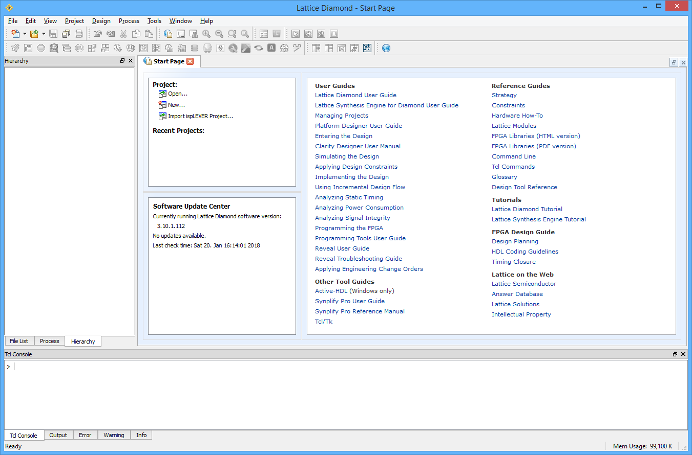
It's the usual sort of thing. There's a large pane for editing files in, a pane to the left shows various views of the project, and a terminal area at the bottom takes output messages from the various programs that operate behind the scenes to do the synthesis and mapping. Here are pictures of the files and process panes:


image


image


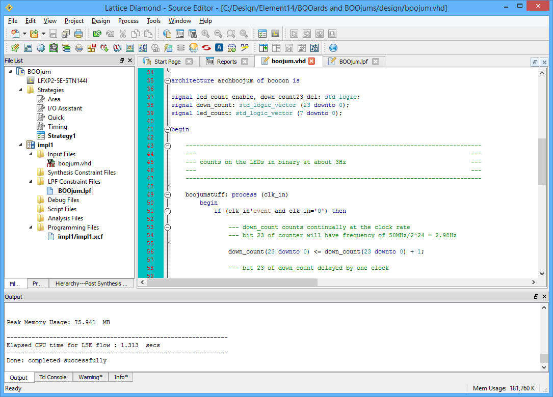
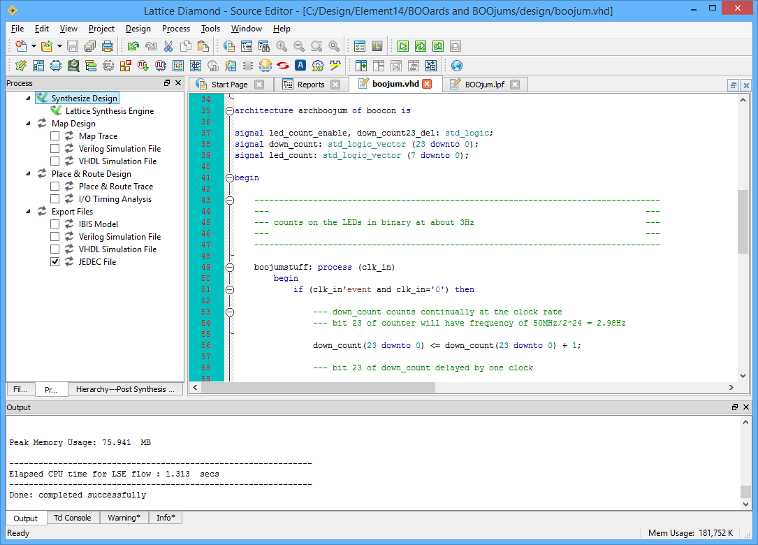
I created a new project (Files->New->Project), setting the destination directory and the part type. Then I selected the files view, left clicked on Input Files, and selected (Add ->New File) to give me a VHDL (.vhd) source file to work with. Double clicking on the filename loaded it into the editing area and I entered my first go at the VHDL to get the LEDs to count. After sorting out a couple of syntax errors where I'd misstyped things, I had a green tick against 'Synthesize Design' on the process pane and then had a go at double-clicking 'Map Design' and 'Place & Route Design'. That all went fine. I then found that I could bring up views of the placement ('Floorplan View' and 'Physical View') using buttons on the toolbar. So I had a design fitted to the FPGA. There was just one snag (there always is a snag somewhere along the way when you're hunting a snark), the mapping didn't know anything about the external hardware on the board and had just randomly assigned the IO pins.


Hmm. There didn't seem to be a tool (that I could see) for setting the pinout, but the files view had a constraints file entry so I looked in the Lattice example project for the board and, lo and behold, there was a .lpf file that had entries for the pins, giving pin numbers and other information. I copied it all to my .lpf file and adapted my VHDL to use the pin names. (I also took the precaution of tying the control signals for the SRAM, SPI memory, and the UART tx line to fixed levels in my VHDL so they would be inactive.) After rerunning the synthesis and mapping, I then found I had a floorplan where the correct pins were being used. (There's probably a better way to set up the pinning than this, so I guess I'm going to have to read the documentation at some point.)


Final step was to see if I could program the FPGA. I ticked the box next to 'JEDEC File' on the Export Files section of the process pane (since that was the only option in view that might serve for programming), double-clicked 'JEDEC File itself and the software then produced the file for me. I hit the Programmer button on the toolbar, changed the settings to use the FTDI programmer, and then hit the program button.


The FPGA was programmed and I saw the LEDs counting. Except I didn't; shame to say, I'd made a mistake in the code and had to go back and rework the VHDL. Then it worked and here's the video to prove it:


You don't have permission to edit metadata of this video.
Edit media
x
image
Upload Preview
image


[1] https://en.wikipedia.org/wiki/The_Hunting_of_the_Snark
[2] http://www.latticesemi.com/en/Products/DevelopmentBoardsAndKits/LatticeXP2Brevia2DevelopmentKit.aspx

  • Sign in to reply

Top Comments

  • genebren
    genebren over 5 years ago +2
    Jon, Excellent write-up. It is rewarding to see something as simple as LEDs counting away, especially when you now how much work (and learning) it took to make it happen. I have to admit, I too am getting…
  • genebren
    genebren over 5 years ago

    Jon,

    Excellent write-up.  It is rewarding to see something as simple as LEDs counting away, especially when you now how much work (and learning) it took to make it happen.  I have to admit, I too am getting the bug to do a little VHDL. And now I understand about Boojumsimage

    Thanks!

    Gene

    • Cancel
    • Vote Up +2 Vote Down
    • Sign in to reply
    • More
    • Cancel
element14 Community

element14 is the first online community specifically for engineers. Connect with your peers and get expert answers to your questions.

  • Members
  • Learn
  • Technologies
  • Challenges & Projects
  • Products
  • Store
  • About Us
  • Feedback & Support
  • FAQs
  • Terms of Use
  • Privacy Policy
  • Legal and Copyright Notices
  • Sitemap
  • Cookies

An Avnet Company © 2023 Premier Farnell Limited. All Rights Reserved.

Premier Farnell Ltd, registered in England and Wales (no 00876412), registered office: Farnell House, Forge Lane, Leeds LS12 2NE.

ICP 备案号 10220084.

Follow element14

  • X
  • Facebook
  • linkedin
  • YouTube