


In this post, I document the firmware I use to test the DAC8775, the subject of the Quad-Channel, Analog Output Module RoadTest.
I'm using a Hercules automotive microcontroller to talk to the DAC. I'll cover the peripheral configuration and the test code. Even if you're using a different controller, the sequence of events may help you to write your own code for this DAC. |
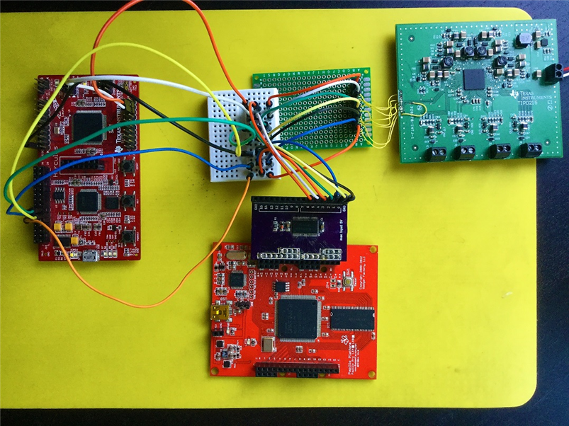
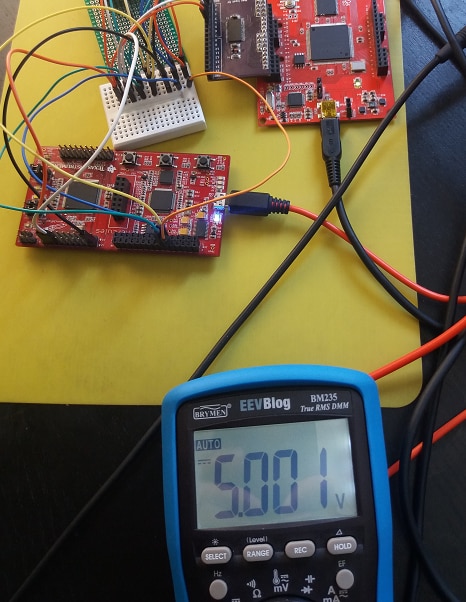
Connections
The Hercules is one of the smallest of the family, a TMS570LS04. I use this because it has all peripherals on board to do this exercise.
It's also my favourite microcontroller. We have a history together.
I'm using two GIO pins for the nRESET (GIO A.6) and nALERT (GIO A.7) signals. The SPI is served by the Hercules' SPI #3.
This choice is because I'm using a LaunchPad, and these pins are easily accessible.
| DAC EVM PIN | Signal | LaunchPad PIN | Signal | Logic Analyser Signal |
|---|---|---|---|---|
| 1 | SPI DIN (MISO) | J10.12 | SPI3.SOMI | 1 |
| 2 | SPI nCS | J10.13 | SPI3.nCS0 | 3 |
| 3 | GND | J2.1 | GND | GND |
| 4 | SPI CLK | J10.11 | SPI3.SCLK | 0 |
| 5 | VDUT | nc | nc | nc |
| 6 | SPI DOUT (MOSI) | J10.14 | SPI3.SIMO | 2 |
| 7 | nRESET in | J2.8 | GIOA.6 | 4 |
| 8 | nc | nc | nc | nc |
| 9 | nALARM out | J2.9 | GIOA.7 | 5 |
| 10 | nc | nc | nc | nc |
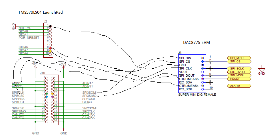
I've connected a volt meter over output A of the DAC board to validate behaviour.
Configure Hercules Peripherals
As usual for this controller family, I configure peripherals and drivers with the HALCoGen application.
Drivers and PINMUX
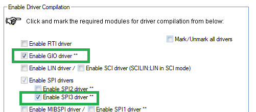
I'm using the GIO driver for the nRESET and nALARM signals. SPI3 is the SPI port of choice.
Take care that alll signals that require MUX setup are active (on the TSM570LS04 they are all active by default. If you're using another Hercules, please check).
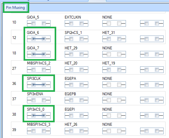
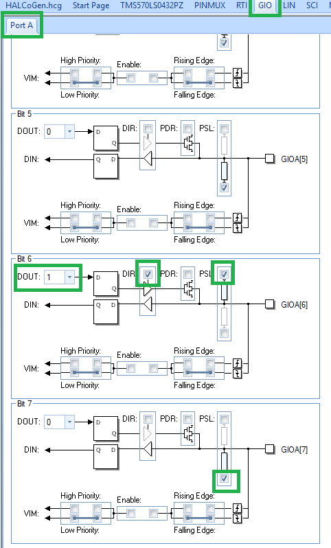
GIO
GIOA.6 is entertaining nREST. Set it as an output port, dafault to 1.
GIOA.7 listens to nALERT. Set it as an input port. Set the pull-down resistor to prevent the pin from flapping in the breeze.
SPI
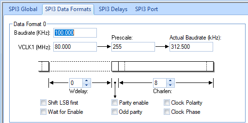
In the data format block, you define the speed (you can up the speed in real life. I'm using a breadboard so I'm restricting it to 321.5 kBaud) and the SPI word length.
This is also where you can define the clock polarity and phase.
In the Port block, you set the functionality of the SPI pins. I've set all that are used to SPI, all the rest to GIO.
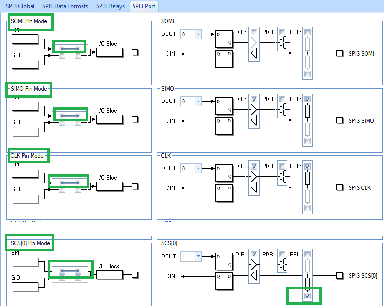
To avoid bogus info in the nCS line, I've set the pull-down. Without thit, I get runt pules (same with MISO).
This may not be neccessary when you'e using a PCB instead of a breadboard and patch wires.
Firmware
Dependencies and Globals
Here the headers of the drivers are added. I've defined constants for the nRESET and nALARM signals for readability.
The buffer for SPI input and output are defined here too.
/* USER CODE BEGIN (1) */
#include "gio.h"
#include "spi.h"

#include <stdint.h>

#define RESET 6
#define ALARM 7


uint16 TX_Data_Master[3] = { 0x00 };
uint16 RX_Data_Master[3] = { 0x00 };
/* USER CODE END */
In the main() function, we first initialise GIO and SPI. At that point. The settings we've done in HALCoGen are applied.
At the end of this block, the DAC is hardware-reset by pulling the nRESET pin low and then back high.
int main(void)
{
/* USER CODE BEGIN (3) */
    uint32_t uLoop = 0U;
    spiDAT1_t dataconfig1_t;

    gioInit();

    dataconfig1_t.CS_HOLD = TRUE;
    dataconfig1_t.WDEL    = TRUE;
    dataconfig1_t.DFSEL   = SPI_FMT_0;
    dataconfig1_t.CSNR    = SPI_CS_0;

    /* Enable CPU Interrupt through CPSR */
    _enable_IRQ();

    spiInit();
// reset the DAC
gioSetBit(gioPORTA, RESET, 0);
// 10 ns needed, the effective time is 610 ns
gioSetBit(gioPORTA, RESET, 1);
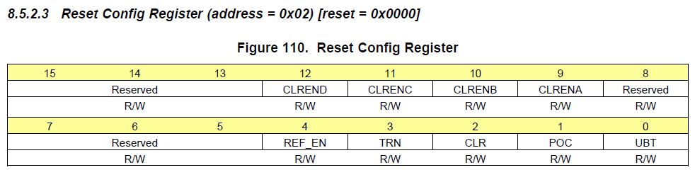
Next step is a software reset.
    // reset
    TX_Data_Master[0] = 0x01;
    TX_Data_Master[1] = 0x00;
    TX_Data_Master[2] = 0x01;
    /* Initiate SPI3 Transmit and Receive through Polling Mode */
    spiTransmitAndReceiveData(spiREG3, &dataconfig1_t, 3, TX_Data_Master, RX_Data_Master);
Then a validation of the communication by writing the user bit and reading it back:
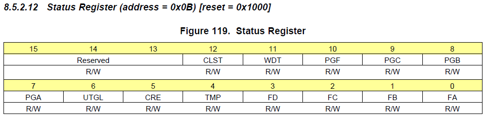
    // toggle user bit
    TX_Data_Master[0] = 0x02;
    TX_Data_Master[1] = 0x00;
    TX_Data_Master[2] = 0x01;
    /* Initiate SPI3 Transmit and Receive through Polling Mode */
    spiTransmitAndReceiveData(spiREG3, &dataconfig1_t, 3, TX_Data_Master, RX_Data_Master);

    // read user bit
    TX_Data_Master[0] = 0x8b;
    TX_Data_Master[1] = 0x00;
    TX_Data_Master[2] = 0x00;
    /* Initiate SPI3 Transmit and Receive through Polling Mode */
    spiTransmitAndReceiveData(spiREG3, &dataconfig1_t, 3, TX_Data_Master, RX_Data_Master);

    // nop should return user bit
    TX_Data_Master[0] = 0x00;
    TX_Data_Master[1] = 0x00;
    TX_Data_Master[2] = 0x00;
    /* Initiate SPI3 Transmit and Receive through Polling Mode */
    spiTransmitAndReceiveData(spiREG3, &dataconfig1_t, 3, TX_Data_Master, RX_Data_Master);
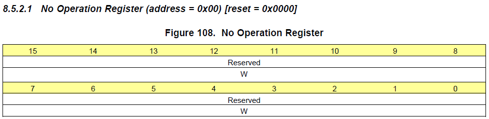
Then the functional part:
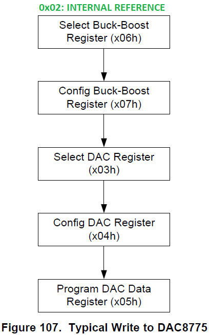
Enable the internal reference. The EVM doesn't have an external one.
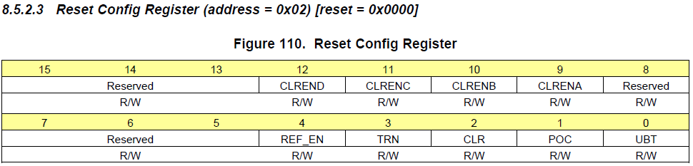
    //
    TX_Data_Master[0] = 0x02;
    TX_Data_Master[1] = 0x00;
    TX_Data_Master[2] = 0x10;
    /* Initiate SPI3 Transmit and Receive through Polling Mode */
    spiTransmitAndReceiveData(spiREG3, &dataconfig1_t, 3, TX_Data_Master, RX_Data_Master);
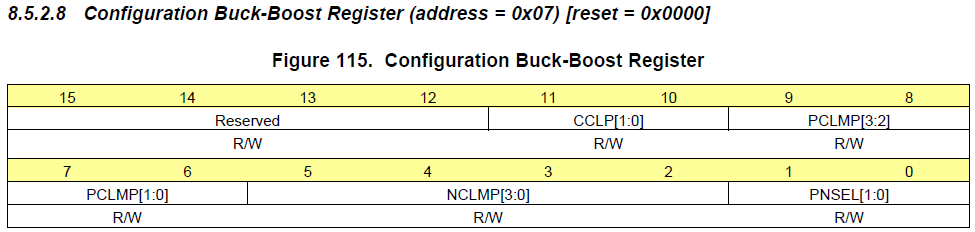
Select and configure the Buck-Boost module:
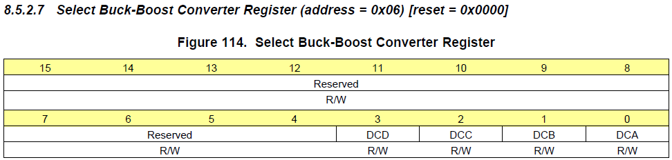
  //
    TX_Data_Master[0] = 0x06;
    TX_Data_Master[1] = 0x00;
    TX_Data_Master[2] = 0x0f;
    /* Initiate SPI3 Transmit and Receive through Polling Mode */
    spiTransmitAndReceiveData(spiREG3, &dataconfig1_t, 3, TX_Data_Master, RX_Data_Master);

    //
    TX_Data_Master[0] = 0x07;
    TX_Data_Master[1] = 0x06;
    TX_Data_Master[2] = 0x1f;
    /* Initiate SPI3 Transmit and Receive through Polling Mode */
    spiTransmitAndReceiveData(spiREG3, &dataconfig1_t, 3, TX_Data_Master, RX_Data_Master);
Select and configure the DAC output
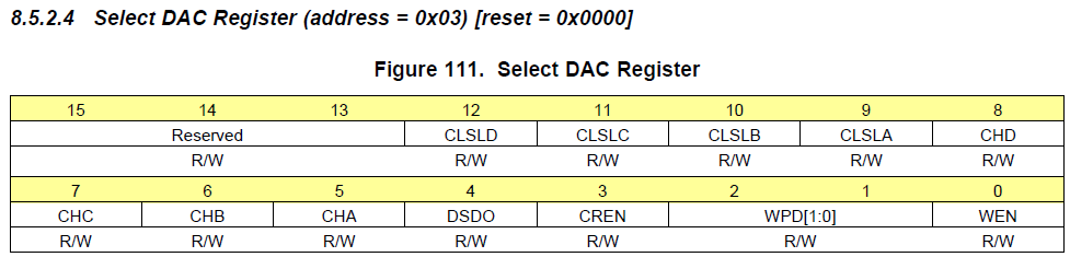
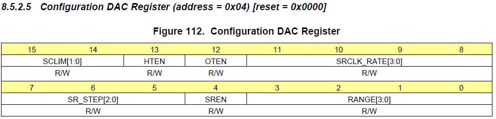
    //
    TX_Data_Master[0] = 0x03;
    TX_Data_Master[1] = 0x00;
    TX_Data_Master[2] = 0xf0;
    /* Initiate SPI3 Transmit and Receive through Polling Mode */
    spiTransmitAndReceiveData(spiREG3, &dataconfig1_t, 3, TX_Data_Master, RX_Data_Master);

    //
    TX_Data_Master[0] = 0x04;
    TX_Data_Master[1] = 0x10;
    TX_Data_Master[2] = 0x00;
    /* Initiate SPI3 Transmit and Receive through Polling Mode */
    spiTransmitAndReceiveData(spiREG3, &dataconfig1_t, 3, TX_Data_Master, RX_Data_Master);
... and finally set the output value.
    //
    TX_Data_Master[0] = 0x05;
    TX_Data_Master[1] = 0x08;
    TX_Data_Master[2] = 0xff;
    /* Initiate SPI3 Transmit and Receive through Polling Mode */
    spiTransmitAndReceiveData(spiREG3, &dataconfig1_t, 3, TX_Data_Master, RX_Data_Master);

    uLoop = 1U;
    while (uLoop) {

    }
/* USER CODE END */
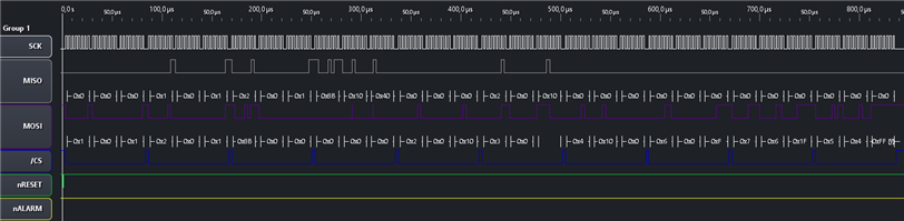
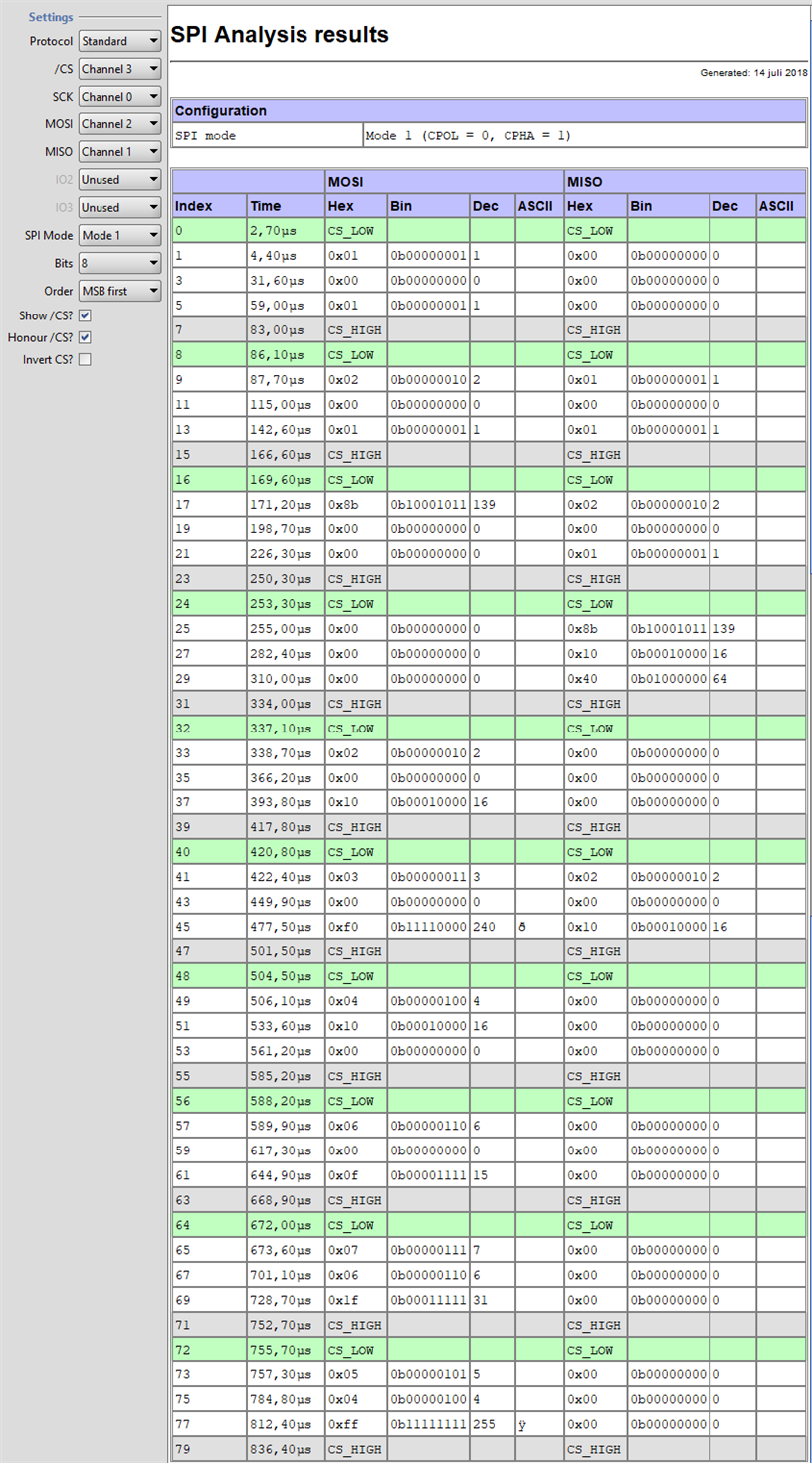
action shot of writing 0xffff to register 0x05
Below is a capture of the sequence. Note that when I took the capture, I had the Buck-Boost and DAC configuration parts switched around.
That's not good, because I enabled the output too soon (when writing register 0x04).
In the next posts I'll review the DAC's functionality.
edit: source code and HALGogen / CCSv8 project files attached
Top Comments