


The world is analogue, although it is best processed digitally. As such, I am often asked what’s the best way to implement the digital processing element? Is it by using a DSP or an FPGA? This blog will discuss this question and provide a pathway to an answer.
Let’s start our discussion with an understanding of what signal processing is. Signal Processing in its simplest form addresses a wide range of applications that analyse, generate, or modify information contained within a signal.
These analysis, generation, and modification techniques are used across a range of market segments from ISM to Communications, Defence, Space, and Consumer applications.
Across these market segments signal processing algorithms are the backbone of applications such as medical imaging, process monitoring and control, Voice and Data Compression, Object Detection, Guidance, Secure Communication, Image / Video processing, RADAR and SONAR, etc.
Typical signal processing techniques used in these applications include Multiplication, Addition and Subtraction, Filtering (moving average, FIR, IIR, etc), Discrete and Fast Fourier Transforms, Convolution, Transforms (e.g. wavelet), Histograms, and so on. When we implement these algorithms digitally, we call this Digital Signal Processing (DSP), and it offers many benefits over an analogue approach.
These advantages include no effects from component tolerances, drifts, or aging. Crucially, a digital approach also offers significant noise immunity when compared to an analogue approach, which uses a continuous signal and is therefore highly susceptible to noise. While a quantised digital signal is not susceptible to noise, we do have to consider the effects such as rounding and truncation have on the signal in its place. For example, rounding in one direction can result in an offset, while truncation can result in accuracy impacts.
To receive and transmit the analogue signals, we use Analogue to Digital and Digital to Analogue Converters, with the digital processing element in the middle (Figure 1).

Figure 1: Basic Signal Processing Chain: ADC, Processing Element, and DAC
When it comes to implementing the digital signal processing, engineers often face a choice of implementing the algorithm in a Digital Signal Processor (DSP) or Field Programmable Gate Array (FPGA). So how are they different, and which one should we choose?
What is the difference between a DSP and an FPGA?
Both FPGAs and DSPs are fundamentally different devices. DSPs are a class of specialised processors which are optimised for implementation of DSP algorithms, particularly Multiply Accumulate (MAC) and repetition. As DSPs are processor-based, they are sequential in nature. That is, each instruction in the program goes through a fetch, decode, and execute cycle (Figure 2). The performance of the DSP is therefore determined by how many clock cycles are required for each instruction. To increase the performance, several DSP cores are often implemented in the same device to allow for parallel operation. Of course, in this architecture common resources such as external memory can also become a bottleneck, as resources are required to arbitrate for access. Such arbitration can affect the responsiveness and determinism of the algorithm being implemented. To further increase parallelism and, hence performance, DSPs can also implement Single Instruction Multiple Data (SIMD) and Very Long Instruction Words (VLIW) capabilities.
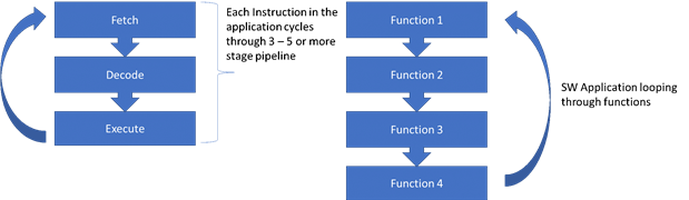
Figure 2: DSP Sequential World
FPGAs on the other hand are not a class of processor; instead, they offer a range of logic resources such as Configurable Logic Cells, Block RAM, DSP elements, etc. (Figure 3) As such, FPGAs are programmed using designs which configure and connect the logic resources to implement the desired algorithm.
FPGA performance is therefore measured by the clock frequency with which the design can achieve timing closure. In an FPGA-based algorithm implementation, each clock cycle could be performing mathematical operations. This frees the FPGA developer from the sequential world found by DSP developers and allows the implementation of signal processing pipelines and parallelisation dependent upon the resources of the device. Traditionally, FPGAs have been considered harder to program than DSPs due to the different architecture and the need to consider timing closure.
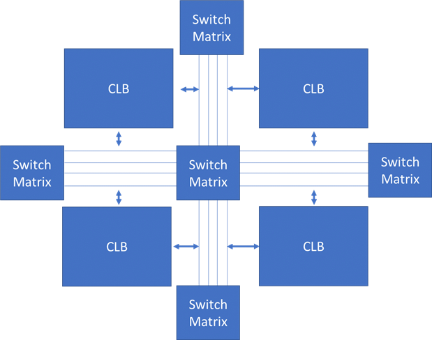
Figure 3: FPGA Architecture
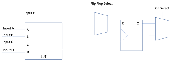
Figure 4: Simplified CLB Architecture
Fixed or Floating-Point Representation
There are two methods of representing numbers within a design: fixed or floating-point number systems. Both DSPs and FPGAs can implement fixed and floating-point number systems.
Fixed-point representation maintains the decimal point within a fixed position, allowing for straight forward arithmetic operations. A fixed-point number consists of two parts called the integer and fractional parts. The major drawback of fixed-point representation is that to represent larger numbers, or to achieve a more accurate result with fractional numbers, a larger number of bits is required. If it is not possible to increase the storage length, then there is a loss of precision. This can occur in a DSP where the size of all vectors is fixed. In an FPGA-based approach, as we are defining the hardware, the vector can be sized to ensure there is no loss of precision or accuracy.
Floating point representation allows the decimal point to float to different places within the number depending upon the magnitude. Floating point numbers are divided into two parts: the exponent and the mantissa. This is very similar to scientific notation, which represents a number as ‘A times 10 to the power B, where A is the mantissa and B is the exponent. However, the base of the exponent in a floating-point number is base 2, that is, A times 2 to the power B. The floating-point number is standardized as IEEE / ANSI Standard 754 and utilises an 8-bit exponent and a 24-bit mantissa. A 32-bit floating-point number can therefore represent a number between ±1.18×10−38 to ±3.4×1038
While DSPs often have inbuilt support for floating point operations, FPGAs are optimised for fixed point operation. As such, implementations of floating-point solutions can impact performance.
Common Performance Metrics
At the heart of many signal processing algorithms is the Multiply Accumulate operation, which is used when implementing Finite Impulse Response (FIR) Filters. The number of Multiply Accumulates which can be performed in a second is therefore often used as an indication of raw performance, and reported as MACS or Multiply Accumulation performed per Second on device data sheets.
Of course, DSPs are also capable of working with floating point numbers; as such the floating-point performance of a DSP is reported as Floating Points Operations per second or FLOPS.
When it comes to performance, FPGAs blow away DSP-related solutions. For example, a Xilinx Virtex XCVU27P contains 12,288 DSP elements. According to the Xilinx Virtex data sheet, each of these is capable of being clocked at 891 MHz Maximum, which gives a maximum MACS of 10,948 GMACs.
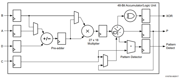
Figure 5: Xilinx Seven Series DSP Accumulator
By comparison, a DSP processor offers performance in the range of hundreds of GMACs (e.g., the 307 GMACs (TI 66AK2H14).
Interfacing
Both FPGAs and DSPs require the ability to interface with high speed Digital to Analogue and Analogue to Digital Converters. Along with the converters, they may also be required to interface with several commonly used embedded system standards such as UART, CAN, I2C, SPI, Gigabit Ethernet, and USB.
Typically, DSPs have support for a fixed number of interfaces. This can limit the selection of remaining system components, as the interfacing capability of the DSP acts as constraint.
FPGAs by their very nature provide flexible IO structures, which provide support for a wide range of single and differential IO standards. For very high-speed links, Multi Gigabit serial links are provided, which can be used with standards such as JESD 204B. These serial links can be used to connect to high speed 100G Ethernet, SATA, PCIe, or USB 3 Interfaces.
Programming DSP or FPGA
DSPs can be programmed using C, or an optimised application assembler. As such, programming is very similar to programming any processor-based solution, although obviously coding styles need to be adjusted to the architecture. As the DSP is also programmed using C branching, and implementing control structures and algorithms is easy in an FPGA, this will require the implementation of a soft processor core or a state machine of varying complexity depending on the branching required.
Traditionally, FPGA development has required in-depth digital design skills, using VHDL or Verilog. Although vendor IP cores are available for algorithms such as FFT, FIR filters and so on, digital design skills have still been required to implement the design. However, High-Level Synthesis (HLS) enables C based implementation of algorithms for FPGAs. This offers several benefits, as the verification of the C Algorithms is much faster than corresponding HDL verification. The ability to use HLS enables the system architects’ algorithms to be used directly. The only thing that needs to be added is the optimisations for programmable logic implementation. (Figure 6)
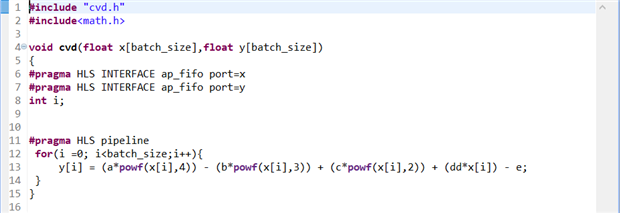
Figure 6: Simple Vivado HLS example of a polynomial equation.
Of course, both FPGA and DSP based solutions can be generated using tools such as Matlab and Simulink; however, the licensing costs can be considerable.
So, which one should I use?
Both FPGA and DSP are tools in our engineering tool box. The correct choice for the application comes down to correct identification of the project requirements, available skill set, and project time lines. However, if you need a solution that’s high-performance, deterministic, responsive, and power efficient, then an FPGA-based implementation is probably the way forward.