


I was recently working on an electronic load - a digitally controlled current sink which could draw a defined current from a power supply regardless of voltage. I had to draw a couple of amps from a 20V supply, with a large bandwidth and high accuracy, so I ended up with the classic linear circuit of an op-amp and a mosfet.

It’s a pretty straight forward design, you feed a voltage into the op-amp (say, from a DAC), and the op-amp will drive the gate of the FET such that the drain current develops a voltage across the shunt resistor. That voltage is then fed back to the inverting input of the op-amp, creating a negative feedback loop, and the current through that resistor becomes proportional to the input voltage. Except of course, the drain current doesn’t come from the input voltage, it comes from the drain. So you can connect the drain to your DUT (i.e, the power supply under load), and control the current drawn mostly independent of the voltage.
It’s a pretty good circuit because the accuracy is very high (basically as good as your op-amp) and the speed is fast if you can drive the MOSFET gate hard enough. I should mention that its pretty power in-efficient, since it basically dumps everything as heat in the MOSFET - If you go down this route for even a modest power dissipation be prepared to dive into thermal management issues. A simple SMPS bench supply wouldn’t think much of 30V at a couple of amps, but trying to remove 60W from a DPAK isn’t straight forward.
So a nice and simple circuit so long as your power is manageable, however there are a couple of nasty surprises waiting to bite your stability if you aren’t careful.
The first is obvious, it’s a circuit that cannot work without another. There is no telling what unsuspecting power supply will be required to suddenly supply several amps worth of heat power to my design, and you have to at least try to make sure that your products will behave sensibly (even when they cant behave as intended) under any imaginable conditions. In reality, those unimaginable conditions really boil down to self preserving behaviour of the power supplies such as over current fold-back, and highly inductive outputs on the power supplies. It’s the second that causes real issues, either from the supply itself (maybe the output bulk capacitors have gone) or from the connections being made via very long wires. In my case, I knew that the wires would be long (deliberately so), so I had to account for a significant inductance in the MOSFET drain
The second is more subtle - we have included the transconductance of the MOSFET in the feedback path of the op-amp, ( or to put it in simpler terms, the voltage-to-current gain of the MOSFET will influence the voltage at the non inverting input). This isn’t necessarily a problem, except that the MOSFET transconductance has a frequency curve (dependence) which changes dependent on the DC operating point.
The third comes in 2 parts and is obvious but ignored. (or at least I ignored it) – the circuit is non linear. Anyone who has studied this sort of circuit should recognize that the current to input voltage linear relationship is dependent on a few things, most obviously that if Vgs falls below Vth the MOSFET turns off and the drain current falls to zero. It doesn’t matter how far below the threshold voltage the gate voltage goes, the drain current remains zero, and we no longer have a linear input to output characteristic. Similarly, if the drain voltage falls low enough that the MOSFET goes out of saturation, or even further so that the body diode is forward biased, the drain current becomes more dependent on the drain voltage than the gate voltage, and we don’t have much control over it any more.
None of this should come as a surprise, we know how to handle these things without fan fare. All three can be dealt with by choosing an allowed range of DC operating points, writing it in big red letters on the first page of the manual, and making sure the circuit will still work of those values are exceeded by 20%. We do this every time we use an op-amp with non-infinite power supply voltages, or calculate the power in a transistor.
For the above limitations, we might simulate a circuit like this:

I’ve chosen parts readily available in LTSpice, except for the MOSFET protection diode, which I’ve modelled as a voltage source plus random Schottky diode. Its not really important to the point I am making, but its required in the circuit to firstly, make the response to inductor flyback a bit more realistic and secondly it just looks wrong to not have a catch diode anywhere near an inductor and a fet. Even though this is not a switch mode circuit, we still expect the current draw to be turned on and off, which means that we still need to provide a path for the inductor to empty its energy through. As for the rest, my choice of parts is only to illustrate the problem. I haven’t thought about any other issues, including temperature, so if you build this circuit as shown it will (amongst other issues) probably catch fire. But the real question is - is it stable? Let’s see how the AC analysis works out.
Stability Theory
(if you are familiar, this all might be a bit boring – skip to the next section LTSpice)
There are loads of ways to analyze the stability of a circuit. You can carry out pole-zero analysis in the ‘s’ domain for either the open loop or the closed loop system, you can look at the Nyquist plot, or you can study the phase and gain margin of the bode plot loop gain. Here, we’re going to look at the bode plot. We can take the relatively simple approach of making sure that the “loop gain” goes below 1 before it inverts by 180 degrees.
The theory is straight forward. You look at the system in the frequency domain, and recognize that the feedback path gets more and more phase shifted compared to the input as the frequencies increase (this always happens for one reason or another). Because the feedback path is fed back and subtracted from the input signal, if that phase shift is ever 180 degrees, then the subtraction becomes an addition. Here’s a standard way of looking at an op-amp circuit from a control theory perspective:

(img courtesy of Analog devices : https://www.analog.com/en/technical-articles/loop-gain-and-its-effect-on-analog-control-systems.html)
It’s the plus and minus of the mixer which relate to the inverting and non inverting inputs of the op-amp, and you can see that the mixer results in a single signal Vin−β×Vout , or the difference between the 2 inputs. This is known as the error signal, and is normally extremely small (remember that an op-amp “wants” to make both of its inputs the same voltage?), but fortunately A0 is very large, and so you get a reasonable Vout=A0×(Vin−β×Vout)
.
Anyway, this is all rather simple until we remember that there’s a frequency dependence, and that multiplication by -1 is the same as a phase shift of 180 degrees. The upshot of that is that if the frequency dependence of β happens to shift the phase by 180 degrees, we have inversion due to the feedback network, and then re-inversion due to the mixer input. That is to say, β×Vout is negative, and so −β×Vout is positive. Our error signal is suddenly much larger because it’s the sum of 2 positive quantities, and A0 multiplies this to give a huge Vout.
So, we effectively have an amplifier with positive feedback! The phase inversion of the feedback network makes the op-amp behave as though we had connected the feedback path to the non-inverting input. This still isn’t quite an unstable system, because the gain of A0 or β could be so small that the signal gets ever more attenuated, or even A0 could include a phase shift at that frequency which counteracts the phase shift due to beta. In reality A0 is more likely to include a phase shift in the same direction as the β phase shift, and so we should consider the 2 together.
The condition for stability therefore is that the gain at that frequency (where the summed phase shifts are 180 degrees) is less than 1, or 0 dB. The gain of course referring to the gain of both A0 and β .
The gain of A0 and β might otherwise be called the gain of everything in the feedback loop, or even the “loop gain” as we have been referring to, and is simply the expression βA0 .
Note that on a log graph, we can go from log(A0×β)=log(A0)+log(β)=log(A0)−log(1β ) But of course, 1β is the closed loop gain! In other words, a log graph of open loop vs closed loop response provides a nice visual for the loop gain:

Image also courtesy of analog devices
If you still are unclear, Matt Duff from ADI has a good video here: https://www.youtube.com/watch?v=oOsltCa7qBo
So there we have it. We simple need to do a sweep of the frequencies, and check that there is no point in the frequency dependent loop gain which has a 180 degree phase shift and a gain greater than 0dB. The distance away from 180 degrees that the response is when it crosses the 0dB line is called the phase margin, and the distance away from 0dB when the phase is -180 is called the gain margin.
This is all straightforward, but There's an even simpler approach which simply requires you to plot the loop gain and check the slope as it crosses 0dB, this is called rate of closure, and is explained in the second part of Matt’s video here:
https://www.youtube.com/watch?v=xvZ7R9rujM4
we will press on with actually measuring the phase margin though, since its easier to get with LTSpice and it’s a more accurate result.
LTSpice Simulation
We can use LTSpice to simulate these things and check the result. We can plot the loop gain in several ways, but the easiest is to break the loop at the inverting input, and plot the difference between the nodes on either side of the break. This method is not completely fool proof, because it relies on there being a high impedance node on one side of the break, however with the input to an op amp on one side of the break, its hard to go wrong. If you really want to be sure, there’s a more complicated method involving a more complicated setup known as the Middlebrook method which doesn’t have this requirement, but its not necessary in this case.
Here’s what the circuit looks like with the loop broken and an AC source added to drive signals around the loop:

what we are essentially doing here, is to try to plot vout/vin for the loop itself (i.e, the classic gain equation). we have to keep the loop connected though, since otherwise the feedback network wont do its job, and the circuit wont resemble the normal operating conditions. so our zero volt voltage source allows us to inject a signal into the loop without compromising the DC operating points because the feedback network is still connected to the inverting input of the op-amp.
another way to plot the loop gain involves adding an inductor so huge it looks open circuit at anything above DC, then injecting a signal into the feedback node via a huge capacitor. essentially setting up a different circuit for the DC operating point analysis.
Anyway, here's the resulting plot:
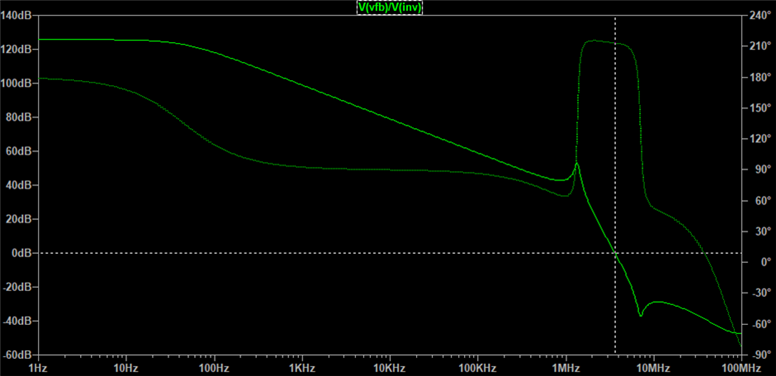
As you can see, the phase margin is large where the gain crosses 0dB, and the circuit is stable. Nice and easy right? Lets just double check it on the transient simulations. Here's the circuit for simulation:

And here’s the step response:

Ah.
Well we know what’s going on here right?
Well, maybe you do, but I didn’t.
when I first came across this, I couldn't understand why all the theory said it should be stable but the transient simulation shows persistent oscillations. I did stability analysis in all the different ways I could think of, eventually deciding that the transient sim was wrong and built it anyway.
of course it sang exactly as LTSpice predicted. I eventually sorted it, by coming up with a good explanation, testing it, finding a fix, proving it in simulation, and finally proving it in the real world. when coming to write this blog, I used the same techniques but it doesn't quite work on this "random parts" circuit, at least, not fully. I'm now starting to doubt myself.
Anyway, Part 2 coming soon … in which ill try my best to explain what's going on, if I can work it out between now and then
please comment if you know / want to guess / want to tell me off for not adding capacitive compensation around the op-amp / have any questions