element14 Community
element14 Community
    Register Log In
  • Site
  • Search
  • Log In Register
  • Community Hub
    Community Hub
    • What's New on element14
    • Feedback and Support
    • Benefits of Membership
    • Personal Blogs
    • Members Area
    • Achievement Levels
  • Learn
    Learn
    • Ask an Expert
    • eBooks
    • element14 presents
    • Learning Center
    • Tech Spotlight
    • STEM Academy
    • Webinars, Training and Events
    • Learning Groups
  • Technologies
    Technologies
    • 3D Printing
    • FPGA
    • Industrial Automation
    • Internet of Things
    • Power & Energy
    • Sensors
    • Technology Groups
  • Challenges & Projects
    Challenges & Projects
    • Design Challenges
    • element14 presents Projects
    • Project14
    • Arduino Projects
    • Raspberry Pi Projects
    • Project Groups
  • Products
    Products
    • Arduino
    • Avnet & Tria Boards Community
    • Dev Tools
    • Manufacturers
    • Multicomp Pro
    • Product Groups
    • Raspberry Pi
    • RoadTests & Reviews
  • About Us
  • Store
    Store
    • Visit Your Store
    • Choose another store...
      • Europe
      •  Austria (German)
      •  Belgium (Dutch, French)
      •  Bulgaria (Bulgarian)
      •  Czech Republic (Czech)
      •  Denmark (Danish)
      •  Estonia (Estonian)
      •  Finland (Finnish)
      •  France (French)
      •  Germany (German)
      •  Hungary (Hungarian)
      •  Ireland
      •  Israel
      •  Italy (Italian)
      •  Latvia (Latvian)
      •  
      •  Lithuania (Lithuanian)
      •  Netherlands (Dutch)
      •  Norway (Norwegian)
      •  Poland (Polish)
      •  Portugal (Portuguese)
      •  Romania (Romanian)
      •  Russia (Russian)
      •  Slovakia (Slovak)
      •  Slovenia (Slovenian)
      •  Spain (Spanish)
      •  Sweden (Swedish)
      •  Switzerland(German, French)
      •  Turkey (Turkish)
      •  United Kingdom
      • Asia Pacific
      •  Australia
      •  China
      •  Hong Kong
      •  India
      • Japan
      •  Korea (Korean)
      •  Malaysia
      •  New Zealand
      •  Philippines
      •  Singapore
      •  Taiwan
      •  Thailand (Thai)
      • Vietnam
      • Americas
      •  Brazil (Portuguese)
      •  Canada
      •  Mexico (Spanish)
      •  United States
      Can't find the country/region you're looking for? Visit our export site or find a local distributor.
  • Translate
  • Profile
  • Settings
Personal Blogs
  • Community Hub
  • More
Personal Blogs
Legacy Personal Blogs More on Quiet-Low I/O Drivers and Ground Bounce
  • Blog
  • Documents
  • Mentions
  • Sub-Groups
  • Tags
  • More
  • Cancel
  • New
  • Share
  • More
  • Cancel
Group Actions
  • Group RSS
  • More
  • Cancel
Engagement
  • Author Author: caroline_teledynelecroy
  • Date Created: 18 Apr 2019 10:07 AM Date Created
  • Views 993 views
  • Likes 3 likes
  • Comments 1 comment
  • inductance
  • teledyne lecroy
  • impedance
  • mcu
  • teledyne
  • lecroy
  • ground bounce
Related
Recommended

More on Quiet-Low I/O Drivers and Ground Bounce

caroline_teledynelecroy
18 Apr 2019

Ground bounce can plague digital I/O lines with bit errors and turn your hair grey trying to uncover the cause in the process. But there is a trick you can use to make the analysis a little easier: using a quiet-low I/O driver as a sense line to reveal the existence, and magnitude, of ground bounce in your system.


As we discussed in our last post on this topic, ground bounce happens when multiple I/O drivers share common Vdd and Vss lines AND return paths are not wide, uniform planes, resulting in higher total inductance in the return path. That inductance, in turn, causes a voltage difference between the ends of the common lead, the polarity of which depends on whether drivers are switching high-to-low or low-to-high at any given time.


image

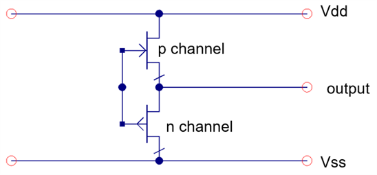
Figure 1: To configure an I/O driver as a quiet-low line, its output is connected directly to Vss on the die


Figure 1 shows us a simple schematic of an I/O driver for reference. Typically, I/O drivers are CMOS devices with p-channel and n-channel junctions that drive the I/O line. We want to fix this driver's output in a low logic state, and to do so, we turn on the n-channel gate in the output and turn off the p-channel gate. We connect the output of the driver directly to Vss on the die with a low-impedance connection.


It's important to bear in mind that, from a signal-integrity standpoint, while we tend to think of interconnects in circuits like these as simple "wires," they actually have electrical properties. In particular, the minuscule return path between the die and the host PCB has a good deal of inductance. But once the return currents of those signal lines reach the solder ball to the ground plane in the board, the inductance of the path to the signal-transmission lines has very low inductance. Once the signal enters the board-level transmission line, the signal and its return propagate on a uniform transmission line. This is what makes it possible for us to use our quiet-low I/O driver to tell us what's going on voltage-wise with Vss on the die vs. Vss on the PCB.


So the key here is that we use one of the I/O outputs as a sense line connected to the Vss rail on the die. We can also make another I/O driver into a quiet-high sense line for the Vdd (or Vcc) rail on the die by doing the inverse, i.e., turning off the n-channel gate and turning on the p-channel gate so that the output is directly connected to Vdd. Then, that output can tell us what's going on with the on-die Vdd rail.


image

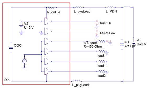
Figure 2: For demonstration purposes, here's how we configured the I/Os on an Arduino MCU


Let's take a look at how this little quiet-low I/O trick is implemented in practice on a  microcontroller (Figure 2). This schematic represents an Arduino MCU that's been instrumented such that there's only one Vcc and Vss connection shared by all of the I/Os. Also, the Vdd, or core-logic power supply, shares the same rail. So, by using a quiet-high for one of the outputs, we can sense not only the Vcc, which is the power supply for the I/O ring, but also the Vdd core-logic supply.


Thus, our quiet-high sense line lets us monitor what's happening with the Vdd rail on the die even as it comes out to a quiet-high transmission line on the PCB, where we have coaxial cables connected to it on the board that bring its signals to an oscilloscope. Meanwhile, a quiet-low I/O driver senses the noise getting through the inductance and resistance of the die's package leads on the die's Vss rail, enabling its comparison to the board-level ground.


For demonstration purposes, one I/O driver serves as a trigger that will switch at the same time as the other drivers. To ensure that the trigger I/O doesn't draw a lot of current, there's a 450-Ω series resistor in that path. From there, the signal is fed directly to a 50-Ω oscilloscope input using a high-bandwidth cable. The two resistances of 500 Ω total draw only about 10 mA from the I/O ring, so that trigger I/O will generate a bare minimum of ground bounce itself. To evaluate the real ground bounce of the switching I/Os, we'll sequentially trigger one I/O at a time, and then both at once.


In an upcoming post, we'll look at the results of our demonstration.


Previous posts in this series:

About Ground Bounce an How to Measure It

  • Sign in to reply

Top Comments

  • Gough Lui
    Gough Lui over 6 years ago +1
    I'm still very much a novice, but it's always nice to pick up these kinds of tips - I'll probably start monitoring the quiet low and global GND to understand the output driver characteristics, while taking…
  • Gough Lui
    Gough Lui over 6 years ago

    I'm still very much a novice, but it's always nice to pick up these kinds of tips - I'll probably start monitoring the quiet low and global GND to understand the output driver characteristics, while taking care to ensure the connection itself doesn't introduce extra bounce. I suspect this could be highly applicable to high-speed FPGAs with many I/O blocks in a complex ... especially if violating the maximum simultaneous switching limits or just wanting to observe simultaneous switching noise. Perhaps in those circumstances, changing certain signals out of certain I/O blocks to other blocks might reduce the impact somewhat.


    - Gough

    • Cancel
    • Vote Up +1 Vote Down
    • Sign in to reply
    • More
    • Cancel
element14 Community

element14 is the first online community specifically for engineers. Connect with your peers and get expert answers to your questions.

  • Members
  • Learn
  • Technologies
  • Challenges & Projects
  • Products
  • Store
  • About Us
  • Feedback & Support
  • FAQs
  • Terms of Use
  • Privacy Policy
  • Legal and Copyright Notices
  • Sitemap
  • Cookies

An Avnet Company © 2026 Premier Farnell Limited. All Rights Reserved.

Premier Farnell Ltd, registered in England and Wales (no 00876412), registered office: Farnell House, Forge Lane, Leeds LS12 2NE.

ICP 备案号 10220084.

Follow element14

  • X
  • Facebook
  • linkedin
  • YouTube