element14 Community
element14 Community
    Register Log In
  • Site
  • Search
  • Log In Register
  • About Us
  • Community Hub
    Community Hub
    • What's New on element14
    • Feedback and Support
    • Benefits of Membership
    • Personal Blogs
    • Members Area
    • Achievement Levels
  • Learn
    Learn
    • Ask an Expert
    • eBooks
    • element14 presents
    • Learning Center
    • Tech Spotlight
    • STEM Academy
    • Webinars, Training and Events
    • Learning Groups
  • Technologies
    Technologies
    • 3D Printing
    • FPGA
    • Industrial Automation
    • Internet of Things
    • Power & Energy
    • Sensors
    • Technology Groups
  • Challenges & Projects
    Challenges & Projects
    • Design Challenges
    • element14 presents Projects
    • Project14
    • Arduino Projects
    • Raspberry Pi Projects
    • Project Groups
  • Products
    Products
    • Arduino
    • Avnet Boards Community
    • Dev Tools
    • Manufacturers
    • Multicomp Pro
    • Product Groups
    • Raspberry Pi
    • RoadTests & Reviews
  • Store
    Store
    • Visit Your Store
    • Choose another store...
      • Europe
      •  Austria (German)
      •  Belgium (Dutch, French)
      •  Bulgaria (Bulgarian)
      •  Czech Republic (Czech)
      •  Denmark (Danish)
      •  Estonia (Estonian)
      •  Finland (Finnish)
      •  France (French)
      •  Germany (German)
      •  Hungary (Hungarian)
      •  Ireland
      •  Israel
      •  Italy (Italian)
      •  Latvia (Latvian)
      •  
      •  Lithuania (Lithuanian)
      •  Netherlands (Dutch)
      •  Norway (Norwegian)
      •  Poland (Polish)
      •  Portugal (Portuguese)
      •  Romania (Romanian)
      •  Russia (Russian)
      •  Slovakia (Slovak)
      •  Slovenia (Slovenian)
      •  Spain (Spanish)
      •  Sweden (Swedish)
      •  Switzerland(German, French)
      •  Turkey (Turkish)
      •  United Kingdom
      • Asia Pacific
      •  Australia
      •  China
      •  Hong Kong
      •  India
      •  Korea (Korean)
      •  Malaysia
      •  New Zealand
      •  Philippines
      •  Singapore
      •  Taiwan
      •  Thailand (Thai)
      • Americas
      •  Brazil (Portuguese)
      •  Canada
      •  Mexico (Spanish)
      •  United States
      Can't find the country/region you're looking for? Visit our export site or find a local distributor.
  • Translate
  • Profile
  • Settings
Personal Blogs
  • Community Hub
  • More
Personal Blogs
Legacy Personal Blogs MOS 6526 CIA as a FPGA
  • Blog
  • Documents
  • Mentions
  • Sub-Groups
  • Tags
  • More
  • Cancel
  • New
  • Share
  • More
  • Cancel
Group Actions
  • Group RSS
  • More
  • Cancel
Engagement
  • Author Author: ajkatz83
  • Date Created: 11 Jul 2018 5:26 PM Date Created
  • Views 2769 views
  • Likes 5 likes
  • Comments 8 comments
  • mos
  • 8-bit
  • xilinx
  • c64
  • fpga
  • 6526
  • commodore_64
  • fpga developement
  • altera
  • logic gate
  • mos technologies
Related
Recommended

MOS 6526 CIA as a FPGA

ajkatz83
ajkatz83
11 Jul 2018

Hello all! It's been awhile since perhaps I have posted anything interesting. There are many projects and such I have on back burns that I eventually want to catch up on, but naturally, when i do want to, something that I use frequently and is of great use to me breaks down, an a diversion begins.


Lately I have been doing for 8-bit computing, mainly with the C64 and SX-64 that I have and refurbished to the best of my abilities. I had recently started up making a Tapuino, which the filesystem and and components work fully thanks to the plans from Peter Edwards! Unfortunately, the one component that I didn't consider carefully was the edge-board connector; not because of the pitch, which was fine at 3.96mm, but that there was a separation in the connector pin from supply voltage and ground that were together, and then all the control pins for red, write, motor and sense. A short occurred for which is that best way to describe it and messed up the CIA #2 chip on the C64 Reloaded I have. I had two spares on hand and that did fix the garbage on-screen when I did power up again. Of course, seeing these are old volatile chips, the replacement spare blew out and I had to use my last spare, aside from spending $50 dollars on ebay for another or a fake one from China.   

Block diagram


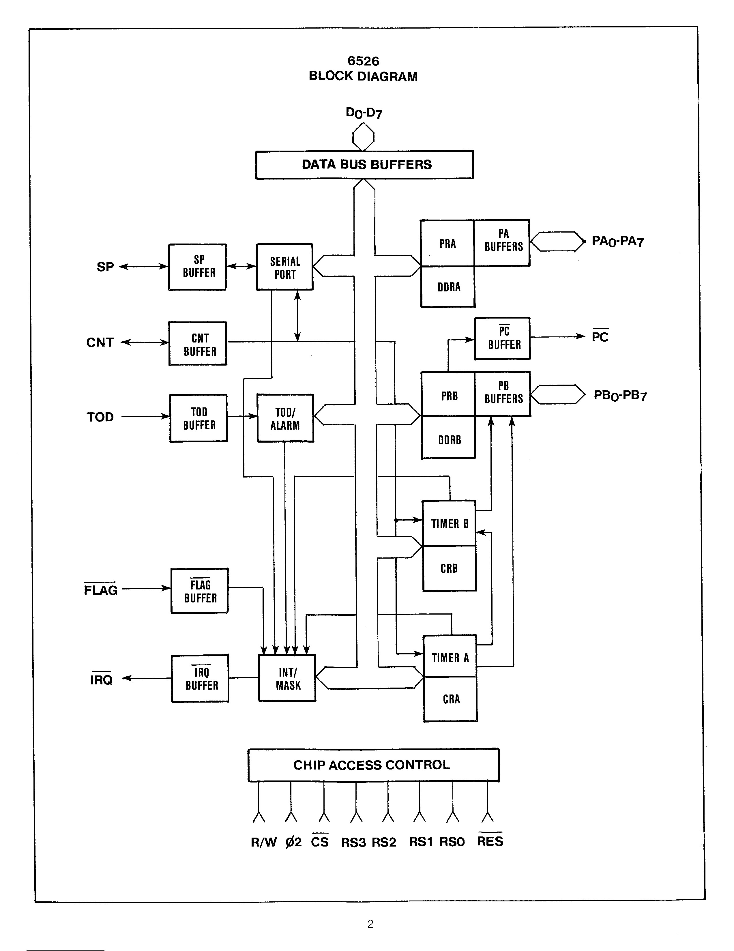
So that is where this block diagram comes into play. In my studies thus far I am getting into digital logic and I had been curious can a so-called "replacement" chip with FPGA development can happen? So far I had got good feedback from a question I did ask and found out that Xilnix Spartan II or Altera Max 10 would be good candidates to make this happen. The issue isn't so much with the FPGA but more so that this block diagram doesn't make as much sense as I would have hoped for. Schematic symbols are relatively easy for me to interpret, however, I am not certain if this here are block logic symbols, or block gate logic symbols--not sure what I am looking at which makes it rather difficult. I assume the squares are registers, the lines in the center are buses? The access control symbols don't mean  much either.


image


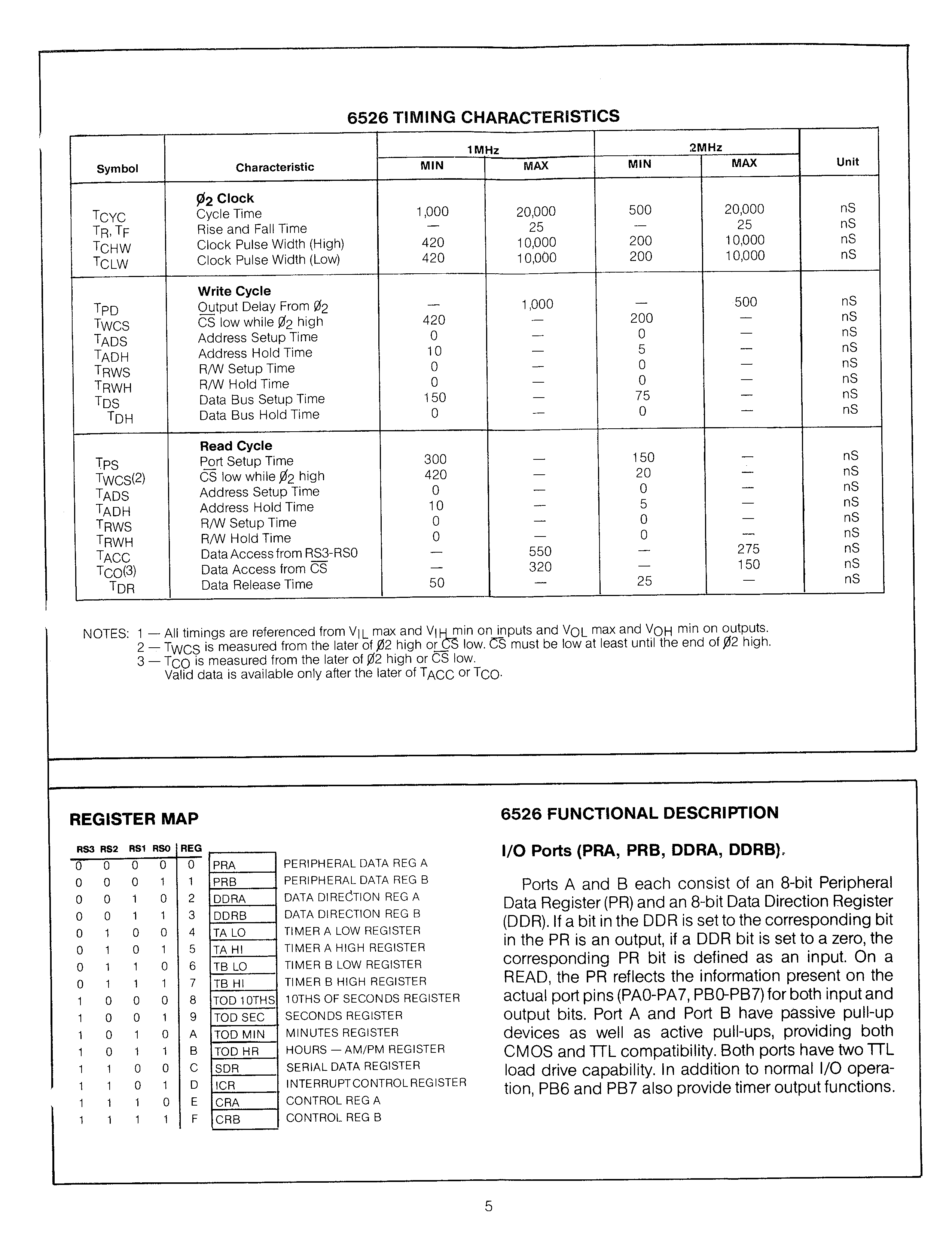
The only thing out of the interfacing section are RS0-RS3 which basically address the register that is being accessed; the truth table that was on one of the other pages made sense as to what those pins did.


I guess mainly how I see all this is not so much in code but rather in a schematic format, meaning, that there should be flip-flops and gates of some kind explaining how this chip functions. I get that it talks about its operation throughout and even on this page, however, seeing it in logic gates interconnected as such just would make more sense to me. Again traditionally, from above, I imagine that the squares are flip-flips and somehow interlinked with NAND gates? I suppose I am confused some may be because there are other devices like the processor and SID that this all interfaces to as well and not knowing how it operates in the entire system has me rather overwhelmed to think how one small piece has its place.


image


I am by no means looking to be spoon fed this, I simply am trying to make sense of this so perhaps I could make some relative replacement and so when this, now 36 y/o technology disappears, some 8 bit machines and still carry on. Just by these two sheets here, I am imagining that I need to concentrate on one pin, as to it's function and find the gate equivalent? Still I am in that schematic design mindset, but that's kind of how I am seeing this all work out.

  • Sign in to reply

Top Comments

  • genebren
    genebren over 7 years ago +2
    Great project. I had to do a similar thing many years ago when a product that our company built relied on an old IEEE controller chip from Intel. We ran out of good choices to procure these chips so we…
  • ajkatz83
    ajkatz83 over 7 years ago in reply to jc2048 +2
    Sorry I didn't get back to you sooner, fell into a funk here, not because of the engineering, just other worldly things. I like what you're saying here. So from the datasheet I have sectioned it out like…
  • jc2048
    jc2048 over 7 years ago in reply to ajkatz83 +2
    When you're developing it, you can do it piece by piece rather than doing the whole design and then trying to make it all work. Indeed it will be better like that. Get a simple bit going first and then…
Parents
  • genebren
    genebren over 7 years ago

    Great project.  I had to do a similar thing many years ago when a product that our company built relied on an old IEEE controller chip from Intel.  We ran out of good choices to procure these chips so we decided to build one from a FPGA.  We had no end of trouble in doing this, as the specifications for the controller did a very poor job of defining all of the signal timing.  In the end, we bailed and bought chips on the gray market (fairly good yield).  But, having said that, if you understand all of the timing and logic, it can be done.


    I have designed glue logic out of CPLD (smaller than most FPGAs) using VDHL to define the logic.  Here are some links to a few tutorials that I wrote on one of those projects.  This should help you to understand how to write logic for some of those blocks in your diagram:

    https://www.element14.com/community/external-link.jspa?url=https%3A%2F%2Fwww.embeddedrelated.com%2Fshowarticle%2F85.php - VHDL tutorial - A practical example - part 1 - Hardware

    https://www.element14.com/community/external-link.jspa?url=https%3A%2F%2Fwww.embeddedrelated.com%2Fshowarticle%2F87.php - VHDL tutorial - A practical example - part 2 - VHDL coding

    https://www.element14.com/community/external-link.jspa?url=https%3A%2F%2Fwww.embeddedrelated.com%2Fshowarticle%2F89.php - VHDL tutorial - A practical example - part 3 - VHDL testbench


    As to some of your other questions on understanding your block diagram, I suggest that you write detailed questions, so people really understand what you are looking for.


    Good luck. We are here to help.

    Gene

    • Cancel
    • Vote Up +2 Vote Down
    • Sign in to reply
    • More
    • Cancel
Comment
  • genebren
    genebren over 7 years ago

    Great project.  I had to do a similar thing many years ago when a product that our company built relied on an old IEEE controller chip from Intel.  We ran out of good choices to procure these chips so we decided to build one from a FPGA.  We had no end of trouble in doing this, as the specifications for the controller did a very poor job of defining all of the signal timing.  In the end, we bailed and bought chips on the gray market (fairly good yield).  But, having said that, if you understand all of the timing and logic, it can be done.


    I have designed glue logic out of CPLD (smaller than most FPGAs) using VDHL to define the logic.  Here are some links to a few tutorials that I wrote on one of those projects.  This should help you to understand how to write logic for some of those blocks in your diagram:

    https://www.element14.com/community/external-link.jspa?url=https%3A%2F%2Fwww.embeddedrelated.com%2Fshowarticle%2F85.php - VHDL tutorial - A practical example - part 1 - Hardware

    https://www.element14.com/community/external-link.jspa?url=https%3A%2F%2Fwww.embeddedrelated.com%2Fshowarticle%2F87.php - VHDL tutorial - A practical example - part 2 - VHDL coding

    https://www.element14.com/community/external-link.jspa?url=https%3A%2F%2Fwww.embeddedrelated.com%2Fshowarticle%2F89.php - VHDL tutorial - A practical example - part 3 - VHDL testbench


    As to some of your other questions on understanding your block diagram, I suggest that you write detailed questions, so people really understand what you are looking for.


    Good luck. We are here to help.

    Gene

    • Cancel
    • Vote Up +2 Vote Down
    • Sign in to reply
    • More
    • Cancel
Children
  • ajkatz83
    ajkatz83 over 7 years ago in reply to genebren

    Hi Gene!


    Well what I was getting at with the block diagram was if the shapes and lines were representative of logic devices (e.g. flip-flops, gates, data buses, etc) because as you mentioned, the documentation of the internal workings of this chip are not too spot on here. While toiling for search terms to give Google, I did come up with a software representation of the CIA 6526 by Wolfgang Lorenz back in 1997 and it's close to what I was thinking of what the internal circuitry on IC might have been. Of course he doesn't account for the serial data port or Time Of Day, but all the timers and registers are shown as interconnected to each other.


    This was his work here:

    https://ist.uwaterloo.ca/~schepers/MJK/cia6526.html 


    I do apologize if it was confusing to read; I was trying to put abstract thought into definable words with the little experience I have here lol. As for the FPGA coding and programming, I'm not going to get impatient and just wait until it gets here. I'll take a look at the links you have provided here and thus far I am getting a tad of handle with what I need to do with ISE software, just what I say was that one can code in VHDL or make schematic in logic gates only (which appealed to me and needed better understanding of the block diagram) than trying to understand VHDL language. I get the feeling I am not going to get around not knowing the VHDL language eh? LOL.  I suppose I am in the research mode at present, CIA 6526 and FPGA wise, and certain things are clicking I believe, I am going to sit down here an actually draw it all out as to what I think is going on.


    So I am sure about:

    • RS3-RS0 being a BCD to access the address register in memory
    • Phi2 is an external clock to the processor phi2 common line (I think that is the 1 or 2MHz clock)
    • DB0-DB7 is just the data bus and goes out to the 6510, so no worries
    • Reset is low until high, and well resets everything lol.

    So far this where I am at, I think more will come as I illustrate a bit tonight!


    Thanks for being there, hard to rattle off idea at times on your own!

    • Cancel
    • Vote Up +1 Vote Down
    • Sign in to reply
    • More
    • Cancel
  • genebren
    genebren over 7 years ago in reply to ajkatz83

    There is quite a bit of detail in the work done by Wolfgang Lorenz.  Apart from the omissions of the TOD and serial ports, I am not sure if I saw any of the logic for the Ports (A&B).  Some of these ideas you might be able to find standalone descriptions (either VHDL or schematic) and use those as a guideline for adding them into your design.


    Good luck!

    Gene

    • Cancel
    • Vote Up +1 Vote Down
    • Sign in to reply
    • More
    • Cancel
  • ajkatz83
    ajkatz83 over 7 years ago in reply to genebren

    O h yes, I do have it all printed out and in front of me. That's presently what I have, ports A and B plus the timers. That's where I am going to make a schematic of some sort.

    • Cancel
    • Vote Up +1 Vote Down
    • Sign in to reply
    • More
    • Cancel
  • jc2048
    jc2048 over 7 years ago in reply to ajkatz83

    The block diagram is high-level and conceptual, it's not meant to tell you how it's implemented. Back then, it was meant to be an aid to understanding for a design engineer using the chip or a programmer understanding what they were doing setting the registers.


    You're in the situation where you're reverse engineering the device. The different blocks will function differently from each other. The ports will  be latches. The serial port will be a shift register, with parallel load and store for the data-bus side and the serial in and out connected to rx and tx. The counters will be, er, counters (carry on like this and I'll earn my engineer's badge).


    You'll need to work in from both sides, on the one hand the register access from the processor buses and on the other back from the IO pins, and try and make it all match up. You've got a reasonably good spec to work with - the datasheet will do a reasonable job of showing you what the chip should do if you get it right. The trickiest bit may well be some of the details of the timer circuits and how they trigger other parts.


    It always used to be the case that you could do a design using purely schematic-capture in Xilinx Webpack, if you wanted, but I'm not familiar with the latest design suites, nor what their competitors allow, so don't quote me on that. If you have the confidence to do this as hardware design with logic, you probably wouldn't find it too difficult to master VHDL.

    • Cancel
    • Vote Up +1 Vote Down
    • Sign in to reply
    • More
    • Cancel
  • ajkatz83
    ajkatz83 over 7 years ago in reply to jc2048

    Sorry I didn't get back to you sooner, fell into a funk here, not because of the engineering, just other worldly things.


    I like what you're saying here. So from the datasheet I have sectioned it out like puzzle pieces and included what pins do what and how they all work. So far the only confusing part was the handshaking with /PC and /FLAG and that all seems to be triggered on negative edges and the /PC just runs for one clock cycle making data ready or accepting it, so I believe.


    Been reading the Write and Reading timing diagrams and there is a lot going on with pulses and such and how fast this is all happening. If I know how to simulate this it would be helpful, seeing I am more visual than comprehending this all abstractly. WIth Xilinx I was watching some videos where it was using their ISE and Webpack was involved where schematics were being created. I have this research from Wolfgang Lorenz which shows the 6526 purely software, except the serial port and TOD. I'm waiting for my FPGA now so I can get my hands on the software and see what I have here in a simulation sense. I believe mostly I am working with S/R flip-flips and something about a decrement counter and some tri-state buffers from the looks of things.


    If I do figure this out I think I should get my engineering badge too LOL. Thanks for your help!

    • Cancel
    • Vote Up +2 Vote Down
    • Sign in to reply
    • More
    • Cancel
element14 Community

element14 is the first online community specifically for engineers. Connect with your peers and get expert answers to your questions.

  • Members
  • Learn
  • Technologies
  • Challenges & Projects
  • Products
  • Store
  • About Us
  • Feedback & Support
  • FAQs
  • Terms of Use
  • Privacy Policy
  • Legal and Copyright Notices
  • Sitemap
  • Cookies

An Avnet Company © 2025 Premier Farnell Limited. All Rights Reserved.

Premier Farnell Ltd, registered in England and Wales (no 00876412), registered office: Farnell House, Forge Lane, Leeds LS12 2NE.

ICP 备案号 10220084.

Follow element14

  • X
  • Facebook
  • linkedin
  • YouTube