


A module is basic building block Verilog. Ports are the interface which module communicate with the environment, in other words, inputs and outputs of the module.
We can assume module as a design box and ports are inputs and outputs of that box. The design box can provide a functionality to higher levels while hiding its internal connection. The analogy reminds me libraries in programming. The following example shows the structure of the module.
module <module_name> (<port_list>);

  ...

  internal_of_module

  ...

endmodule
Verilog module can be described in four levels of abstraction. The method you use doesn't affect the usage of the module. It will appear as a functional box from outside. The inside can use any design methodologies at the end all will be translated to boolean equations.
These design methods are:
Behaviour and Algorithmic Level
This is the most abstract level of the hardware design. It is similar to C language programming.
Dataflow Level
In this level, the designer specifies the data flow.
Gate Level
This design is achieved by describing logic gates and interconnections between them.
Switch Level
This is the lowest level of abstraction. A module is defined with switches, storage nodes, and interconnection between them.
Let's give an example to a module. The example will be an implementation of 74F08 Quad 2-Input AND Gate.
/*
* Program: implementation of 74F08 (Quad 2-Input AND Gate)
* Version: v1.0
* Autor: Mehmet Bozdal
* Date: 1.10.2017
*/


module ic_74F08 (A,B,O);

  //input output decleration
  input [3:0] A;
  input [3:0] B;
  output [3:0] O;

  //internal connection
  assign O = A & B;


endmodule
The module_name is ic_74F08 which has inputs A and B and output O. The only connection is done by assign keyword. Assign is the continues assignment statement. It is used only for modelling combinational circuits. You can also use logic gates which are described in Verilog functions. In that case, assign O = A & B; should be replaced by and(O,A,B) which is gate level modelling.
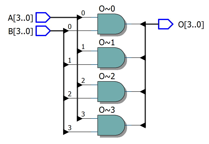
The RTL view of the design is the same as the datasheet of 74F08.
The video above shows how the design work on actual FPGA board. In order to upload your code to FPGA, you can follow instructions on your board's user manual. It is already defined step by step on DE0 Nano's user manual.
I said modules can be used to provide a functionality to higher levels. The process is called instantiation and the module created is called instance. Imagine you need two 74F08 in one design. You can instantiate our previous design and use it more than once. I need to warn you we are not calling a function here. We create actual hardware and each instantiation is a real hardware implementation.
/*
* Program: instantiation of 74F08 (Quad 2-Input AND Gate)
* Version: v1.0
* Autor: Mehmet Bozdal
* Date: 1.10.2017
*/


module ic_74F08_double (Ain,Bin,Out);

  //input output decleration
  input [7:0] Ain;
  input [7:0] Bin;
  output [7:0] Out;

  //instantiation of icle_74F08 module
  ic_74F08 first_74F08 (Ain[3:0],Bin[3:0],Out[3:0]);
  ic_74F08 second_74F08 (Ain[7:4],Bin[7:4],Out[7:4]);

endmodule
The instantiation is done by writing module name followed by instance name and connections of the module. The instance name is not compulsory but it is good practice to give a name. [7:0] Ain is an eight-bit vector. Ain[3:0] is least significant half of that vector.
If we look at the RTL view of the design, there are two identical ic_74F08 design. They have different inputs and outputs.
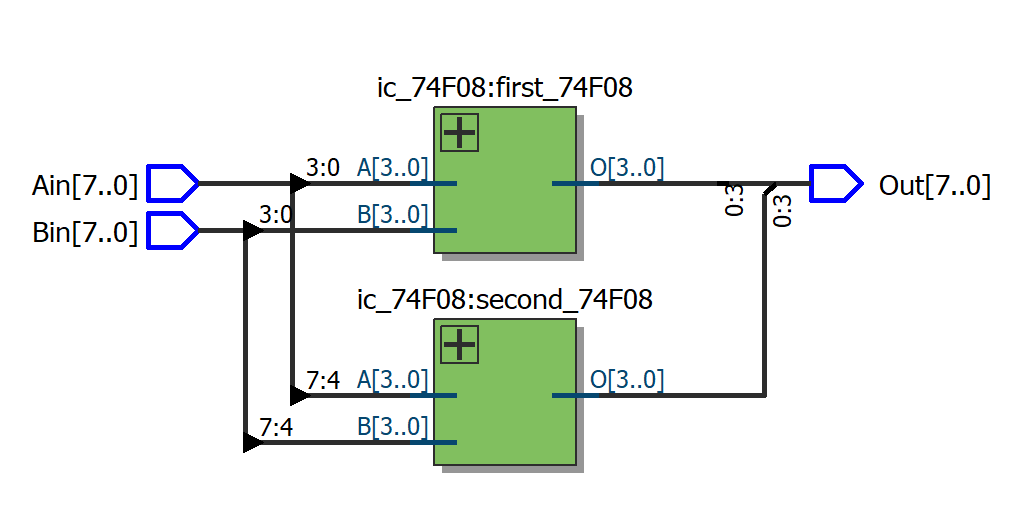
The RTL view of the design has two ic_74F08 boxes which are explored in the previous RTL view.
To see My Verilog Diary you can search for my_verilog_diary or go to the initial article My Verilog Diary - 0 : Introduction. If you have any question, please comment 
Top Comments
-

djfraz
-
Cancel
-
Vote Up
+1
Vote Down
-
-
Sign in to reply
-
More
-
Cancel
Comment-

djfraz
-
Cancel
-
Vote Up
+1
Vote Down
-
-
Sign in to reply
-
More
-
Cancel
Children