


1. What is the need?
With the society beginning to attend more STEM outreach events aimed at school children its important that our members are easily recognizable. Lanyards provide a very easy way to stand out in a crowd. The inclusion of the OLED display is hoped to attract the attention of young people and actively engage with them about electronics as we are finding less and less children are taking up electronics at a secondary school level. We feel this is due to the lack of any substantial practical electronics in the classroom, therefore if we can interest kids at a younger age we hope that more or them will take up electronics.
2. The Project Specification
The Society intends to create a credit card sized ID card to be worn at events. The final design must;
1. Be credit card sized
2. Weigh less than 50 grams
3. Be easily attached to a standard lanyard
4. Incorporate a display
5. Be re-programmable
6. Allow for additional expansions
7. Be ethical
3. The Circuit Design
With the design requirements being the limiting factor we set about work to provide solutions for each of the 7 points mentioned in section 2.
3.1 Power supply design
Our main concern was obviously the weight of the project, as we planned on wearing the lanyard for extended periods of time if we made it to heavy it would quickly become uncomfortable. The main weight of the project would come from whatever portable power supply was used. We had to rule out solar power fairly early on as most of the time we don't have the very bright conditions that we would need to use such a small array. We also didn't wish to use heavy 9V or AA/AAA cells. This left us with somewhat of a dilemma as we knew we needed a 5V stable supply to power our microcontroller, but lighter options couldn't provide 5V on their own. The solution was to use a CR2032 coin cell and a boost converter. This will allow a greater voltage output than the 3V stated.
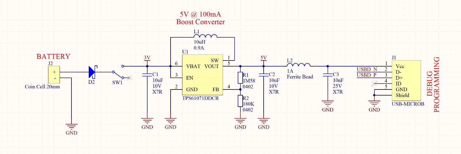
Figure 1.0 - Power Supply with reverse bias protection and boost converter
As seen from Fig. 1.0 we also included a USB port to allow for programming and debugging. This also must share the 5V power line for standard USB protocol, hence why it is included in this schematic block. Although we opted to use SMD components the design could easily be recreated with THT components as all the values are listed.
3.2 Integrated Circuits and Complementary Circuitry
Our integrated circuits choice was relatively simple, as we wanted as small a footprint as possible and an open source hardware package, so we went for an arduino style chip, namely the ATMEGA328P-AU , again any standard ATMEGA 'arduino' chip can be used, the pins will just need slightly reconfigured. We also had to get this to communicate with the USB port for debugging purposes. Although it is possible to interface UART directly to the USB this would have required a significant amount of c code to be created something that we wished to avoid. In order to avoid the lengthy coding time we instead opted to use a FT232RQ this is an IC designed for UART to USB communication as can be seen in Fig. 1.1.
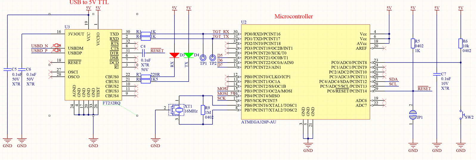
Figure 1.1 Integrated Circuits and supporting Circuitry
The additional supporting circuity can be found on the relevant data sheets, although is included in the schematic (Fig. 1.1).
3.3 I/O
With the Integrated circuits chosen and it was simply a matter of connecting the inputs and outputs. We had selected an OLED with an I2C driver incorporated, this made interfacing with the ATMEGA very easy with only two pins being used as shown in Fig. 1.3, however it wasn't all plain sailing as we will discuss later. There were two other main IO blocks, a 2x3 header to allow the bootloader to be burned onto the ATMEGA chip and an additional empty header to allow for later modifications, such as a Bluetooth module or a speaker.
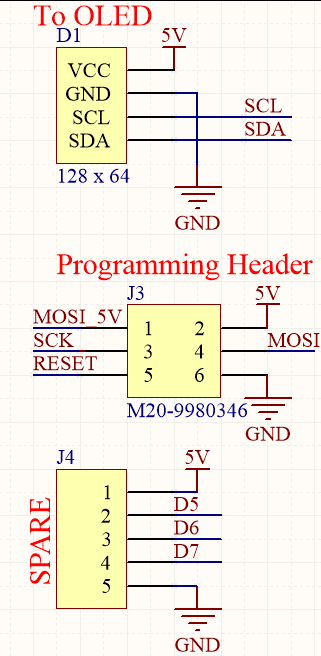
Figure 1.3 IO headers
4. Breadboard Prototyping
With the schematic finalised and checked we began some breadboard testing, this is mostly as a form of sanity checking.
As seen in Fig. 1.4 the power supply was changed, this was done only for testing purposes as the proposed boost converter was untested at this point and was therefore unreliable. A LM7805 linear regulator was used for the test bed as any this would easy any later fault finding.
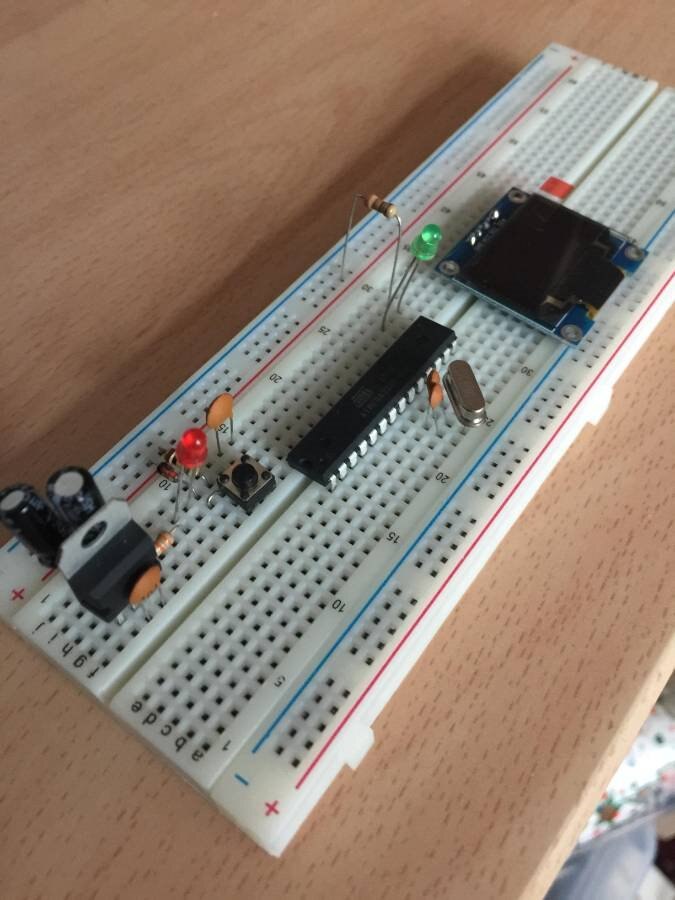
Figure 1.4 - Testing the initial circuit, all components placed and awaiting connections
NB the alternate power supply
At this stage we can across a significant problem, the display didn't seem to work. After testing voltages across the four I2C pins we could see the positive and negative connections were fine. We then probed the data and clock lines and saw the expected intermittent voltage spike which signifies the data transfer. After a lot of frustration it was realised that the I2C display was missing the required pull up resistors needed to operate, with that issue addressed we moved forward.

Figure 1.5 The Full Schematic
5. PCB Design
With the final schematic verified it was time to move onto the PCB design, this was completed in Altium designer 17 (Students can apply to get the software for free). This was simply a case of creating a PCB from the .sch file becoming only a matter of connecting the dots, at this stage it was noted that the the size of the PCB could be significantly reduced, however this was not completed as the credit card sized PCB is more in keeping with traditional ID cards. Altium also let us export the PCB design into a CAD package (SolidEdge- again free for students) to see how it would look in the real world as shown in Fig. 1.7.
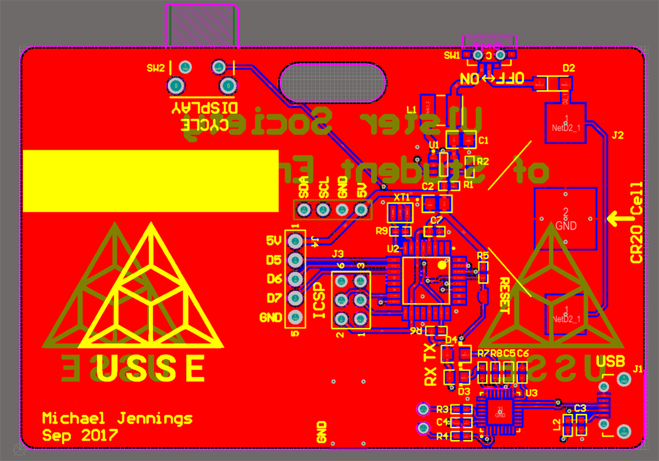
Figure 1.6 PCB design
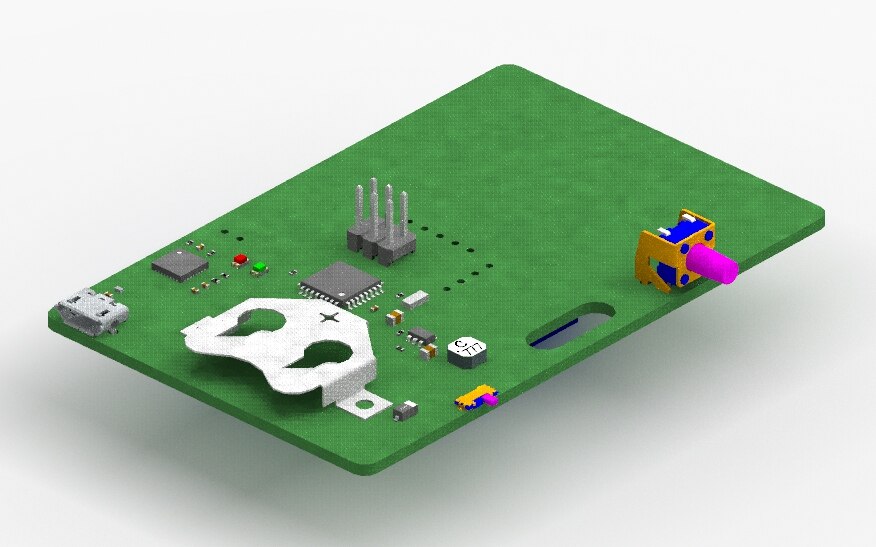
Figure 1.7 A Keyshot photorealstic Rendering of the final design
Environmental Concerns
One of the things that we outlined in our specification was that the design must be ethical, when we ordered our PCB's we had the choice to have them manufactured with or without the use of lead. Although having them manufactured with lead is far cheaper it would also cause problems if we ever needed to dispose of the PCB's due to the dangers of heavy metals such as lead contaminating water supplies. This increased the cost of each board by roughly 1/3 however the society members felt the price increase was justifiable as non-leaded PCB's pose much less danger to the environment.
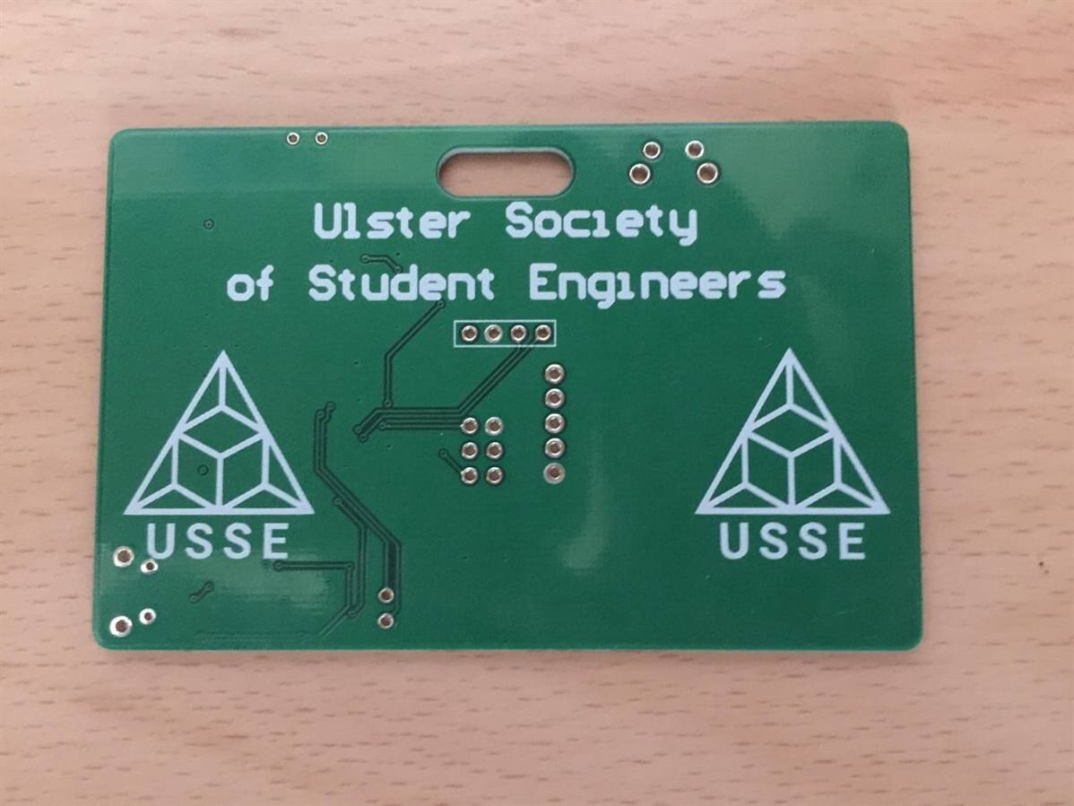
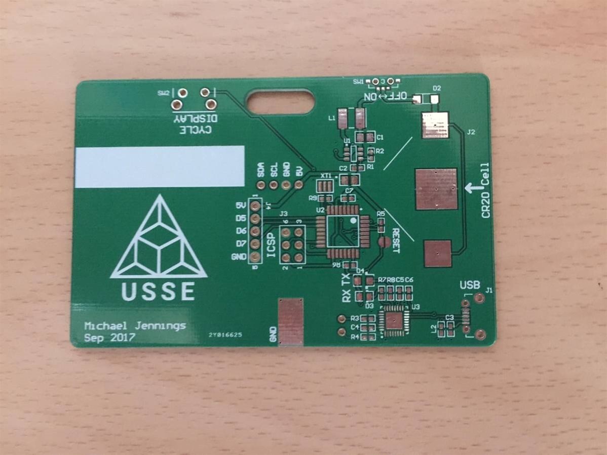
Figure 1.8 Top and Bottom view of the un-populated non-lead PCB
6. Manufacture
With the PCB and components arrive it was time to break out the soldering iron and populate them. The two IC's were the first items to be soldered. Solder paste and a heat gun were used as this is far easier than regular soldering techniques. The rest of the components were hand soldered into place. For the smaller SMD components such as capacitors and resistors a fine soldering tip was used and a pair of tweezers is also advisable. The only component that gave use any trouble was the coin cell battery tab. The tab acted as an excellent radiator and was struggled to find an iron with a high enough thermal mass to properly solder it. Preheating the area with a hot air gun worked, however care must be taken to not de-laminate the solder pads.
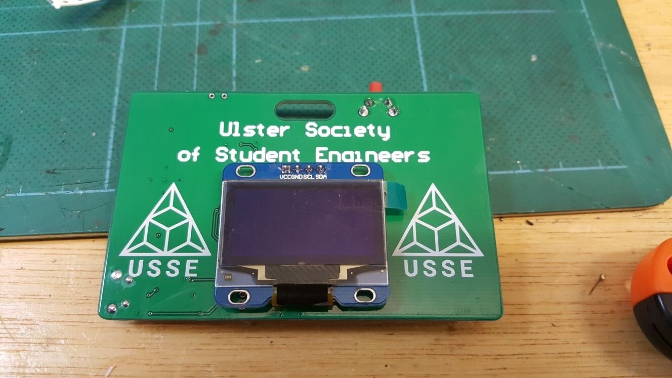
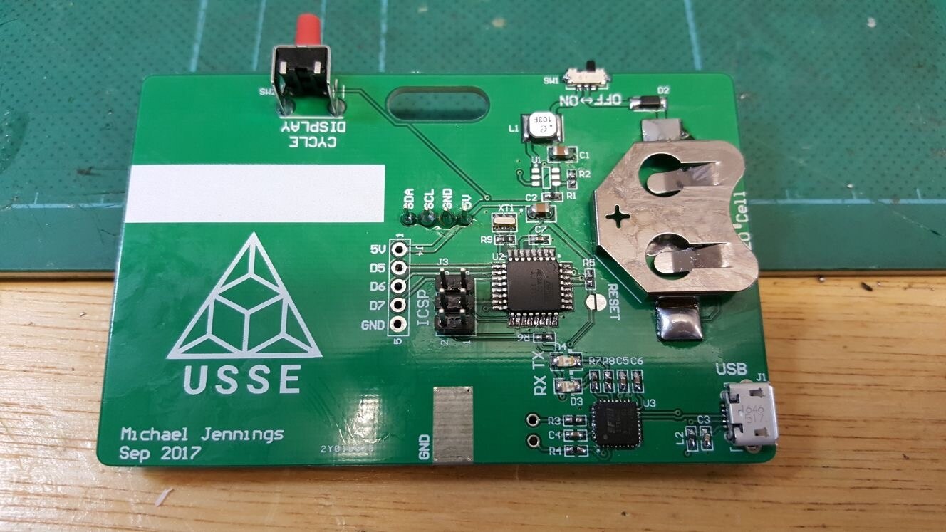
Figure 1.9 The final populated PCB'S
7. Completion and Further Discussion
Specification
In order to measure the success relative to our initial specification its important to ask if the final design meets all requirements. The final design;
1. Is credit card sized
2. Weighs 35 grams
3. Can be attached to a standard lanyard
4. Incorporates a display
5. Is re-programmable via USB
6. Allows for additional expansion in the form of a 5 pin header
7. Does not use lead in its production
The final design therefore meets or betters the initial specification.
Further Discussion
The final design can be seen if Fig. 1.10. One of the great things about the design is that is can use any I2C display module, as can be seen in Fig. 1.9 and Fig. 1.10 two different display modules have been used. this could alternatively be swapped out for any other 4 pin I2C display, the use of an additional header means that nothing even has to be de-soldered. Also with the additional IO header sound or light could be incorporated, this will prolong the life of the product and ultimately make it more useful and marketable.
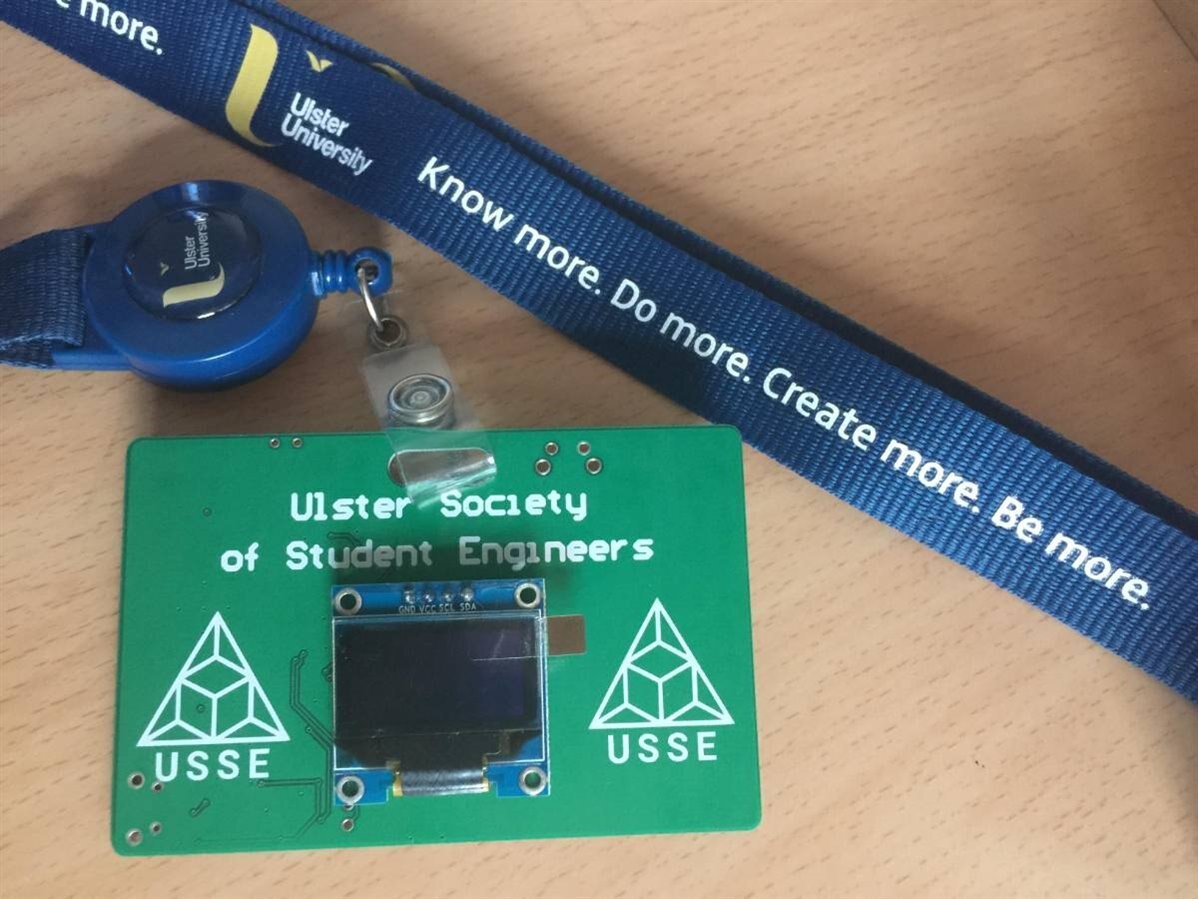
Figure 1.10 The complete design
The one performance statistic that we would like to improve is its battery life. Current high spec CR2032 cells have a comparatively huge internal resistance (circa 20 ohm) this effectively means that 1V is lost across the battery itself. One potential improvement is to include a solar array however with the small surface area and additional circuity required it could use more power than it creates. This is something that we look into and possibly produce a revision b depending on our results.
Using the expansion header it would be possible to incorporate Bluetooth or RF communication into the card, this could allow for interactions between cards in close proximity which could be a fun way to get more people interested in what is going on, interacting with one device and seeing a wireless response on a separate device could be a great way to show the capabilities and gain interest at our STEM outreach events.
Bill of Materials
Please see table 1.0 for required parts list.
| Designator | Description | Manufacturer 1 | Manufacturer Part Number 1 | Supplier 1 | Supplier Part Number 1 | Quantity | Supplier Subtotal 1 |
| C1, C2 | Capacitor | MURATA | GRM21BR71A106KA73L | Farnell | 2611944 | 2 | 0.775 |
| C3 | Capacitor | MULTICOMP | MC0402B103K250CT | Farnell | 1758924 | 1 | 0.034 |
| C4, C5, C6 | Capacitor | TDK | C1005X7R1H104M050BB | Farnell | 2525048 | 3 | 0.426 |
| C7 | Ceramic Capacitor | MURATA | GRM155R71A104KA01D | Farnell | 1828860 | 1 | 0.08 |
| D1 | OLED LCD Display Module, 128X64, I2C IIC Serial, 1.3" | Supplier disabled | Supplier disabled | eBay | 282358769160 | 1 | |
| D2 | Schottky Rectifier, 20 V, 500 mA, Single, SOD-123, 2 Pins, 320 mV | STMICROELECTRONICS | STPS0520Z | Farnell | 1467545 | 1 | 0.0918 |
| D3 | SMD LED RED | KINGBRIGHT | KPT-2012EC | Farnell | 2099236 | 1 | 0.1935 |
| D4 | SMD LED GREEN | KINGBRIGHT | KP-2012LSGC | Farnell | 2463991 | 1 | 0.3065 |
| J1 | USB, SOCKET, TYPE B, SMT | MOLEX | 105017-0001 | Farnell | 2293836 | 1 | 0.366 |
| J2 | Coin Cell 20mm | KEYSTONE | 3002 | Farnell | 1650693 | 1 | 0.594 |
| J3 | Header, 3-Pin, Dual Row, 2.54mm Pitch | HARWIN | M20-9980346 | Farnell | 1022231 | 1 | 1.09 |
| J4, JP1, TP1, TP2 | 5W SIL 2.54mm, Solder Jumper - 2mm, Test Point, 1mm Diameter, Test Point, 1mm Diameter | 4 | |||||
| L1 | Inductor | COILCRAFT | LPS4018-103MRB | Farnell | 2408105 | 1 | 0.748 |
| L2 | Ferrite Bead 200mA 10R@100Mhz 0.025RDC | MURATA | BLM15PG100SN1D | Farnell | 2443233 | 1 | 0.308 |
| R1 | Resistor | VISHAY | CRCW04021M58FKED. | Farnell | 2141062 | 1 | 0.283 |
| R2 | Resistor | MULTICOMP | MCWR04X1803FTL | Farnell | 2447116 | 1 | 0.032 |
| R3, R4 | Resistor | MULTICOMP | MC00625W040211K | Farnell | 1358043 | 2 | 0.063 |
| R5 | Resistor | MULTICOMP | MCWR04X1001FTL | Farnell | 2447120 | 1 | 0.028 |
| R6 | Resistor | MULTICOMP | MCWR04X1002FTL | Farnell | 2447096 | 1 | 0.031 |
| R7 | Resistor | MULTICOMP | MCWR04X2200FTL | Farnell | 2447136 | 1 | 0.026 |
| R8 | Resistor | MULTICOMP | MC00625W040211K5 | Farnell | 1358047 | 1 | 0.011 |
| R9 | Resistor | MULTICOMP | MC00625W040211M | Farnell | 1358123 | 1 | 0.076 |
| SW1 | Slide Switch, SPDT | ALPS | SSAJ120100 | Farnell | 2056803 | 1 | 0.39 |
| SW2 | SPST Tactile, PTH, Right Angle | ALPS | SKHHLSA010 | Farnell | 2056829 | 1 | 0.111 |
| U1 | DC-DC Switching Boost Step Up Regulator, Adjustable, 900mV-5.5Vin, 1.8V-5.5Vout, 0.6Aout, SOT-23-6 | TEXAS INSTRUMENTS | TPS61071DDCR | Farnell | 2144319 | 1 | 1.22 |
| U2 | AVR 8-Bit 32kB 20MHz 32-Pin TQFP | MICROCHIP | ATMEGA328P-AU | Farnell | 1715486 | 1 | 2.5 |
| U3 | Interface Bridges, USB to UART, 1.8 V, 5.25 V, QFN, 32 Pins, -40 °C | FTDI | FT232RQ | Farnell | 1146033 | 1 | 3.56 |
| XT1 | Crystal Resonator 16MHz | MURATA | CSTCE16M0V53-R0 | Farnell | 2443265 | 1 | 1.475 |
Table 1.0 Bill of Materials
We hope you liked the project, let us know if you make your own!
- Ulster Society of Student Engineers
Created 17/09/17 by
Christopher McCausland
EDIT
8. The Code New
We began to code the project, we started by using a Github repository form Olikraus ( https://github.com/olikraus/u8g2/ ). This is an incredibly useful resource as it contains the applicable interfacing code for U8g2 and U8x8 displays, making the project 'plug and play' with any display that utilities either of these display protocols.
As can be seen in Fig. 1.11 the code fist needs to be edited by un-commenting (deleting the '//' at the start of the row) the communication protocol that you wish to use. The Society wished to use I2C protocol as discussed earlier to allow for easy interfacing with the AT Mega.
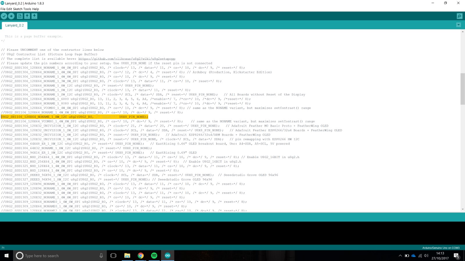
Figure 1.11 - The source code constructor list
After this the code can be broken into two sections.
- Boot and test - Boots the display and tests its fuctioning
- Display code - Drives the display to show what we want.
The boot and test code can be viewed in Fig. 1.12. The code first sets analog input (A0) as an active input and should it be pressed the 'currentState' (what is currently displayed on the OLED) is changed to 'nextState'. These 'States' can be seen in Fig. 1.13 as basic text to be displayed. The numbers before the 'name' and 'role' indicate the offset (in pixels) from the left and top of the display to start each line.
This can also be manipulated to include rolling text and graphics.
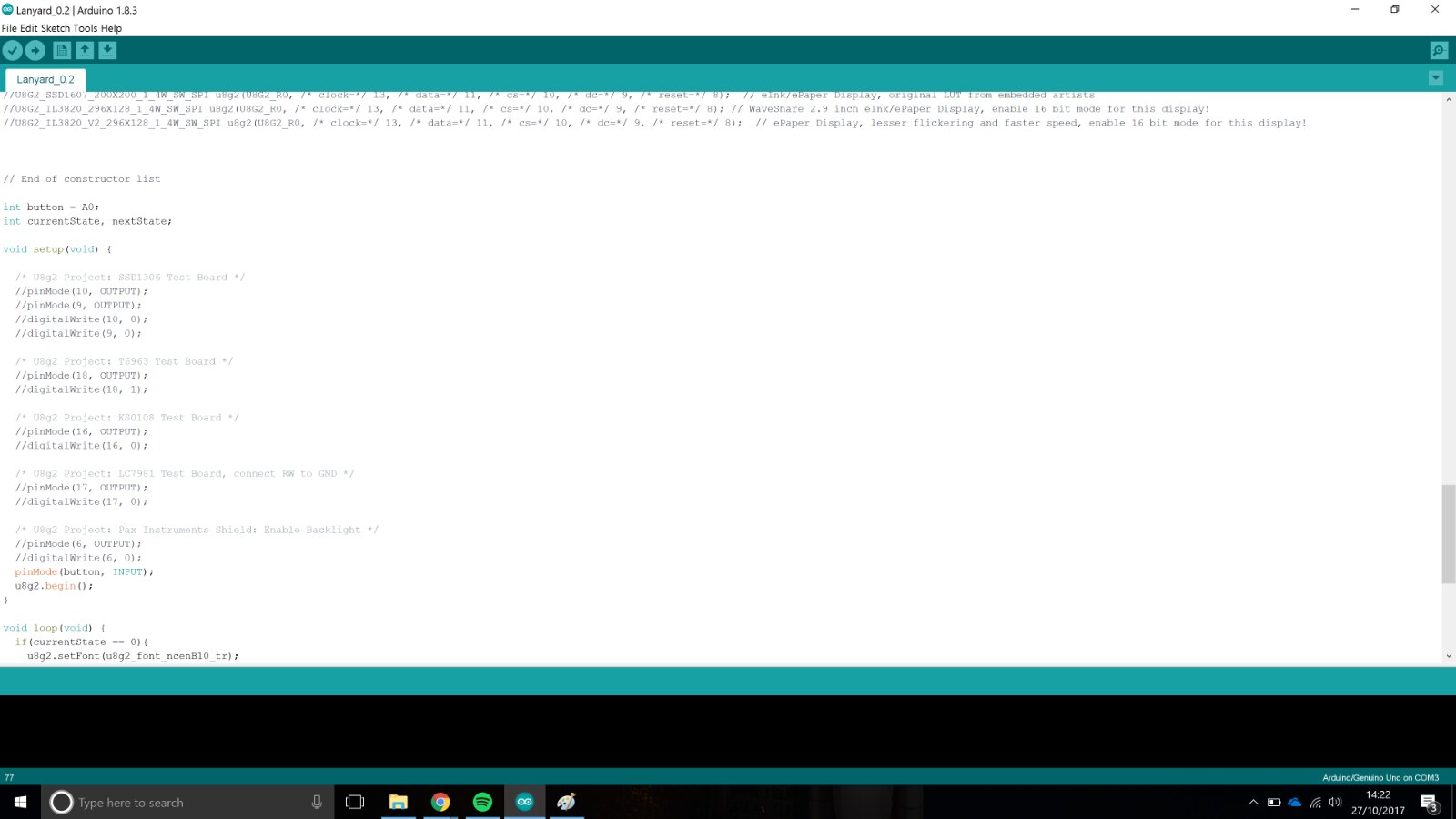
Figure 1.12 - Boot and Test code
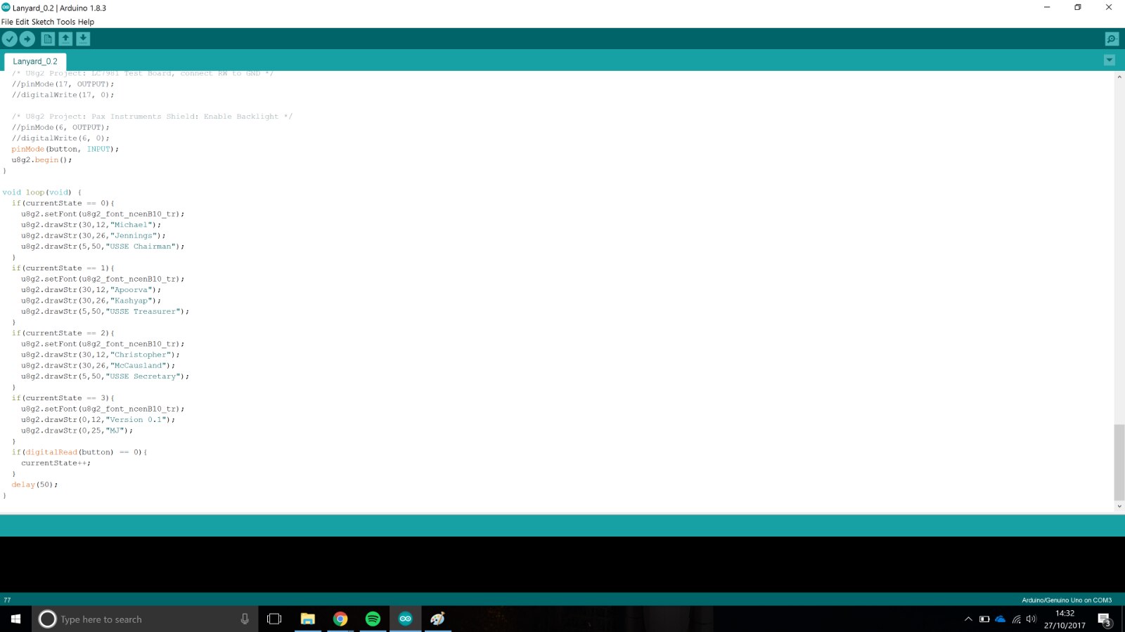
Figure 1.13 - Display code
The code be edited very quickly which should make it highly engaging.
Fig. 1.14 shows the final product in display state 1. After having the project out and about it has received a lots of commendation and interest. The project has therefore been a huge success as it fulfills its task of engaging a wider audience in electronics and particularly resonates with children who have a fascination about seeing the inner-workings of electronics.
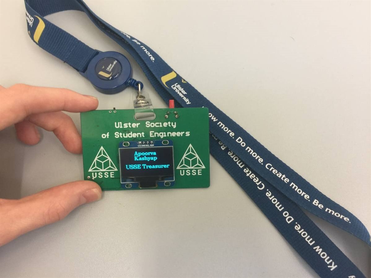
Figure 1.14 - The Final Product
We hope you liked the project, let us know if you make your own!
- Ulster Society of Student Engineers
Created 17/10/17 by
Christopher McCausland
Top Comments