

Ok, so you’ve got a marvellous idea for your next electronic project and you are in the process of bringing together the associated circuitry. You’ve hand-drawn your design on a paper and now you want to make it into a proper schematic file for more analysis, debugging etc. Where do you go? Tada..There’s Circuit Studio from Altium for your rescue. With this tool, you can quickly generate schematics, re-use over 30000 component libraries – schematic + footprint + 3D models, define custom tracks widths, generate layered PCB’s, 3D models..OMG and what not.
Get your free 30-day trial license on element14 and get going today. This blog should help you in getting started with a basic PCB in 20mins or less. OK, on your marks, get-set, go...
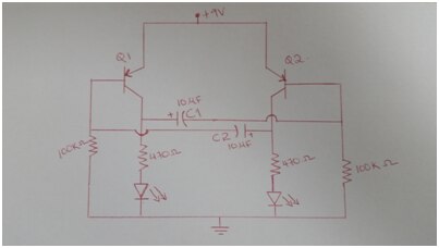
Get your “paper made” design. I’ll use a simple LED flasher based on transistors shown below:
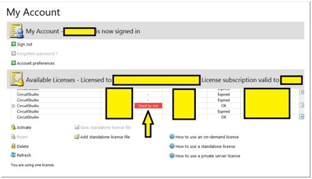
Now, start up Altium Circuit Studio and make sure you atleast have a trial license from element14. You can check this from Help → About → My Account. It should look something like this:
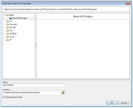
Start a new PCB project from File → New project → PCB project. I’ll choose a “Blank PCB project” type and give it a name “LED_Flasher”.
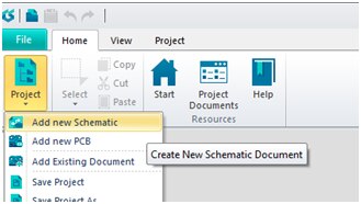
We’ll now proceed to add a new schematic file into this project to “draw up” our circuit on an A4 size sheet. Click on “Project” and “Add a new Schematic” into the project.
Once you have the blank schematic in your project, it’s time to set some options for “Grid size”, “sheet details” etc. Let’s go ahead and do this. Click on the “Project” tab on the top & on the Ribbon menu (i.e. the one that populates when you click on “project” tab), click on “Document Options”. A window showing you all the options for the schematic opens up like below. Set the “Snap grid” to 10 mil for now.
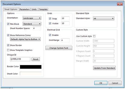
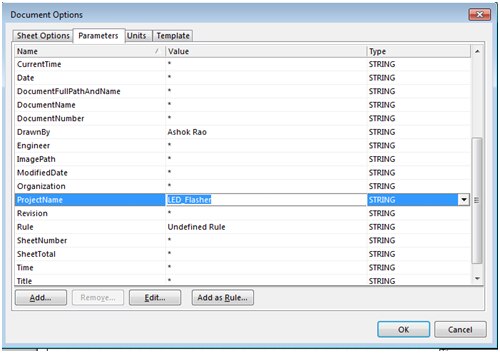
If you want to set other document parameters such as “drawn by”, “modified date” etc, go ahead and enter these as strings in the “Parameters” tab. If you want to set standard units to be used across the breadth of the schematic, set these in the “Units” tab. Once you are satisfied with exploring the options, hit “OK”. My document options look like this:
Now, right click on your schematic in the project explorer and save the file with a name of your choice. Once saved, it’s time to place some parts. The parts we need are:
- PNP Transistor – BC557
- Resistors – 470Ohm, 100KOhm
- Capacitors – 10 uF
- LED – Red, 2x
- A connector for a battery.
Altium Circuit Studio gives you access to Altium’s Vault where over 30000 components have already been listed with schematic, PCB footprint and 3D models for use. We’ll search for our required components in the vault and drag-drop the required ones onto our schematic.
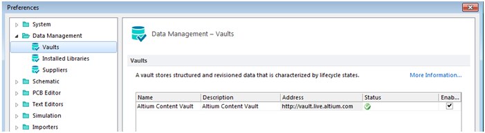
Oh, and by the way, if a vault is not installed already with your installation, you can manually add a vault from File → System Preferences → Data Management → Vaults → Add Altium content vault and use this URL: http://vault.live.altium.com and tick the “Enable” box. Like this below:
Now, you can “consume” the vault content. Open up the “Vault explorer” from the “File” menu. Type in BC557 in the search box and you should see all matches. Click on Transistors folder and select the most appropriate one you feel is OK for your design. I have chosen my best match and what I see is below:

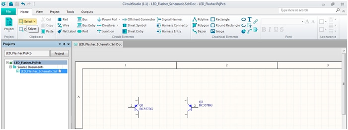
Now, drag-drop the component into the schematic. Directly from the vault. Go ahead and drop 2 as we need 2x for our design. Similarly, find the other components required for the design from the vault and drag-drop onto the schematic file. My schematic looks like this. To get the part designators (Q1, Q2 etc) and set the orientation of the components, double click on the component to open a dialog box where all these parameters can be configured. I’ll now go ahead to drag-drop all the remaining components from the vault and my local library.
To access the local library, right click on an empty space in the schematic, go to “Place part” and click on “Choose”. This will open up the locally installed libraries on your machine. You can also use this for any parts you need.
OK, if you are done, it should look something like this. The 9V and GND are “Net labels”. I found the connector as “Header 2-pin” in the local Miscellaneous Connectors library.

Now, save the project and click on “Project” under “Home” tab, then click on “Options”. On the “ECO generation” tab of the window that opens up, make sure all options have a green tick next to them and click “OK”.
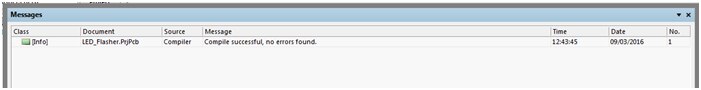
It’s time to compile the project. Click on “Project” under “Home” then click on “Compile”. If there are no errors, you will not see any further windows. However, just to make sure, go to the “View” tab and click on “Messages”. You should see something like this below:
Yippee!! No errors in the design. It’s now time to move on to the PCB stage in Part 2 of this blog.