


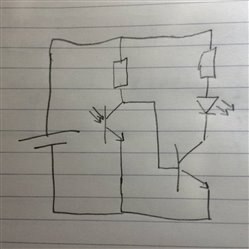
In Part 1 of this series of blog posts, I explained how I got from a hand sketch of a circuit to a schematic in Eagle, CadSoftusa 's PCB Design Software.

This blog takes the randomly placed components onto a board, to the final layout.
This symbol on the top toolbar of Eagle switches from schematic to board view. If a board has not been generated from the schematic already, it asks if you'd like to do this.
First item is to run an Electrical Rule Check (ERC) to make sure there are no electrical errors with the schematic.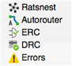
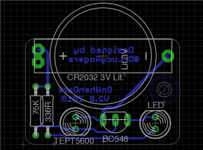
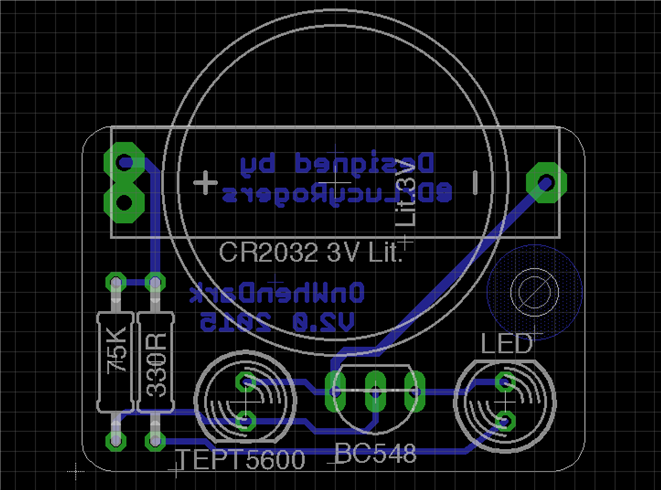
On the board there is a cross in the bottom right hand corner of a wire rectangle. The rectangle is the outline of the PCB, the cross the origin.
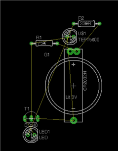
Using the arrows icon move the devices (components) around on the board until you are happy with their placement. The yellow lines that join them indicate which tracks need to be laid between the components.
Right clicking when placing a component rotates it through 90 degrees.
Remember to "save all" at regular intervals.
Holding down the "alt" key changes the grid size to the "Alt" grid. You can check the grid size and Alt size by clicking View, Grid.
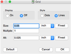
I have it (and I believe the default is as above) so that Alt halves the grid size, allowing you to get things closer together.
You can also make the PCB smaller by moving the wires or clicking the "info" button , clicking on a wire and changing the coordinates.

You can separate the name/value from the component by using the "smash" button - this allows you to move the name of the part onto the PCB in a place where it can be read if required.
PCB's are much more user-friendly if they have holes through which you can mount feet or tie a cable tie. Add a hole using the "add a hole" icon.
You can either make the radius correct to start with, or you can place the hole and edit it using "info" later. I use a 3mm size drill, (the grid is probably still in inches, so you may need to type the "mm" after the 3.) I could maybe have made the drill size 3.1mm to give a bit of clearance for a 3mm screw.

A hole can then be used to screw the PCB down - but you have to leave a space for the screw head. If a screw is tightened down on some tracks, it can cause them to break or short - so it is best to avoid.
You can either avoid the area manually, but there is a nifty trick in Eagle that allows it to be checked in the Design Rule Check (explained later).
Add a circle then edit it using the info button.
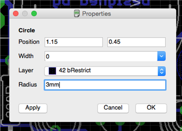
The position should be the same as the hole position. The width needs to be zero - this tells the software that the whole area should be hatched (this is not intuitive).
Place it on the 42 bRestrict layer, and the head of a screw to fit through a 3mm hole will be about 6mm (3mm radius).
Now comes, for me, the most fun part. Joining all the tracks between the components, without crossing over and trying to get it all one sided. (Two sided boards can be made, but they are often more expensive, and also can't be easily made "at home".)
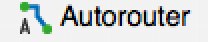
For small boards, I use the "route manually" button rather than the Autorouter as I can control exactly what goes where.
Click on one component to start, then join it to another component. When it has joined correctly, a little noise (low beep) is made. Take care: it is possible to make them look as though they are joined, when they have not quite connected.
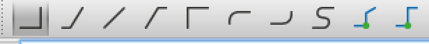
"Best Practice" says that the tracks should be at 45 degrees or 90 degrees as it looks neat. However, as phil.s said in a comment to one of my previous blogs "Electrons don't much care about angles". You can change the angles the track lays by using these buttons:
Thicker tracks are more robust and less likely to "lift" than thinner ones. I have used 0.6mm wide tracks from the battery terminals and 0.4mm wide tracks everywhere else. As this circuit only draws milliamps, this is sufficient. If more current is used thicker tracks are very important.
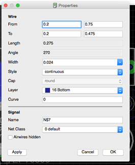
All the tracks are on Layer 16 Bottom.
Once all the tracks are laid, you can check by clicking on Ratsnest . At the bottom right a comment will appear "Nothing to do" if they are all connected as per the circuit diagram.
I then run the ERC (Electrical Rule Check) and the DRC (Design Rule Check) to check for errors. If a track is laid too close to the edge, or too close to another track, it will tell me here. You can change the settings and rules. I approved two rule violations in this board: 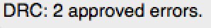
The two positive pads for the battery holder overlap - but as they are both positive, this is what they should do.
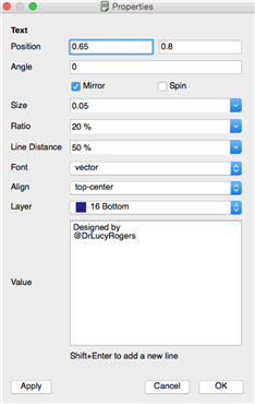
Now all rules have been checked (or apporved), time to add some words - it's nice to rummage through my box of electrical bits and be reminded what is this PCB for, rather than trying to work it out by reverse engineering. I also put the version number, date and my name (you never know, someone may have a fun project they want me involved with ...).
I add words using the text button, then change size and ratio and make the font "vector". This is because I have put it on the 16 Bottom layer - and it will be etched in the copper layer, so it has to obey the same rules as the tracks. If these aren't changed, there will be a DRC (Design Rule Check) error.
Remember to "save all" at regular intervals.
After all of this, I miter the corners - I don't want to stab myself when rummaging in the electronics bits and bobs box. I do this last as I have not worked out how to "undo" it.
Click on the "miter wires" button then change the radius at the top to about 0.05 (inches). Then left click on the wire (edge of PCB). Do this for all the corners.
I save and run all Ratsnest, ERC and DRC again, just to make sure.
And there is my PCB - all done and ready to send of to a manufacturer. However, many manufacturers like to receive PCB designs in a standard file format - called Gerbers.
The next blog will describe how to save the Gerbers - and (hopefully) include some pics of the manufactured board.
I'd be interested to hear your comments - did you use this blog to make a PCB? Was there anything that requires clarification? Do you do things differently?