


Continuing on from the previous PYNQ-Z2 Workshop blogs, this blog continues to investigate the topics covered in the Element 14 PYNQ-Z2 Workshop series led by Adam Taylor, where we took an introductory look at the PYNQ-Z2 development board produced by the Tul Corporation.
In this blog I explore using PS GPIO (EMIO) from within Jupyter Notebooks to interact with logic designs implemented within the FPGA fabric.
The motivation for this started a while back when I was looking at introductory level FPGA design tutorials using HDL languages such as Verilog and VHDL. After encountering many long debates over Verilog vs VHDL and what was the best device family to start with and who the best authors were, etc. I then encountered the problem that each set of recommended training materials tended to target a different trainer or dev board, each with varying numbers of LEDs, switches and LED 7-segment displays. Not only does this quickly get expensive, but some of the recently revised books were targeting boards which were now discontinued.
I already had access to a PYNQ-Z2 dev board, however compared to some of the trainer boards it has a rather limited set of on-board switches and LEDS, a total of six of each, whereas some of the training resources required up to sixteen in order to follow along with. I could have wired in additional user interface hardware to the various Arduino, Raspberry Pi and PMOD ports and then create device constraint files in order to map them appropriately to mimic the trainer boards but instead I started to look at how the PYNQ framework could be used to provide an alternative solution to this problem by moving the physical switches, buttons, LEDs, etc. commonly found on trainer boards onto a software-based user interface. This would allow the various HDL training content to run on the ZYNQ hardware and then customisable layouts in Jupyter Notebooks running on the microprocessor core to handle the user interface.
The first step was to get more familiar with GPIO within the PYNQ framework. I created some simple logic gates (AND, OR, XOR, NOT) in Verilog to simulate entry-level training content and turned then into reusable custom IP blocks to allow then to be used within the Xilinx Vivado tools block design alongside the ZYNQ IP required to create a PYNQ overlay. In the second workshop we had touched on this by using high level synthesis to recreate IP from another overlay but this would be my first attempt at creating a new Verilog design and using it with the PYNQ framework.
Starting the design in Vivado
First off I needed to create the logic gates to be used as basic training content. This was done using some Verilog.
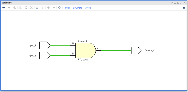
AND gate:
`timescale 1ns / 1ps
module and_gate(
    input Input_A,
    input Input_B,
    output Output_C
    );

// Port definitions
// Description of the digital system
// Dataflow modelling
assign Output_C = Input_A & Input_B;

endmodule
OR gate:
`timescale 1ns / 1ps
module or_gate(
    input Input_A,
    input Input_B,
    output Output_C
    );

// Port definitions
// Description of the digital system
// Dataflow modelling
assign Output_C = Input_A | Input_B;

endmodule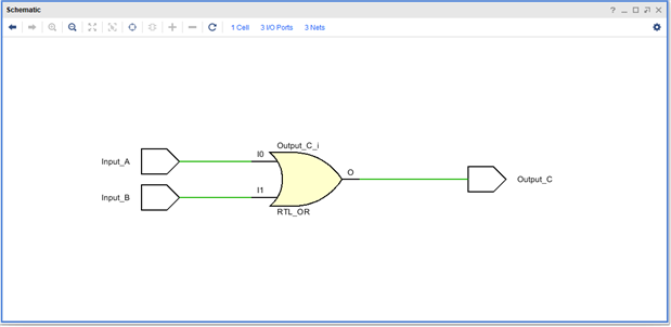
XOR gate:
`timescale 1ns / 1ps
module xor_gate(
    input Input_A,
    input Input_B,
    output Output_C
    );

// Port definitions
// Description of the digital system
// Dataflow modelling
assign Output_C = Input_A ^ Input_B;

endmodule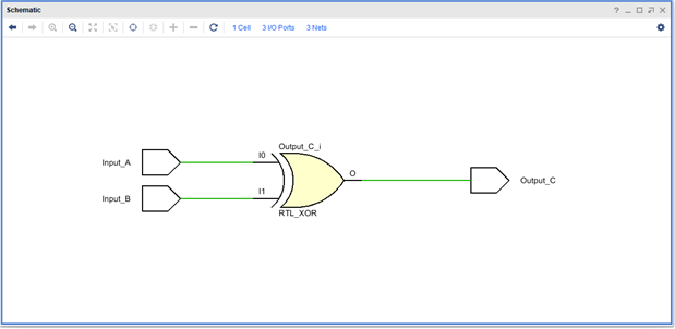
NOT gate:
`timescale 1ns / 1ps
module not_gate(
    input Input_A,
    output Output_B
    );

// Port definitions
// Description of the digital system
// Dataflow modelling
assign Output_B = ~ Input_A;

endmodule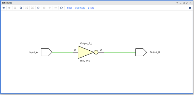
The RTL schematics which Vivado produced all appeared to match what I was expecting. The next step was to get it connected to GPIO.
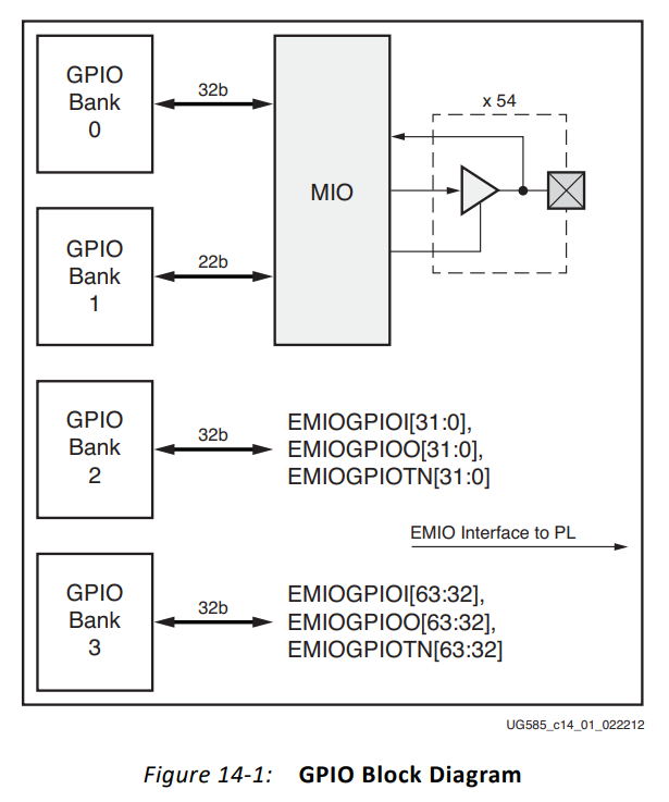
In order to connect the logic gates to the PYNQ framework I decided to use the PS GPIO of the ZYNQ device. The GPIO is divided between two banks of MIO and two banks of EMIO as shown in the Xilinx UG585 documentation:
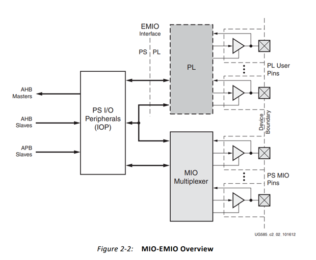
The two EMIO banks provide the interface between the PS and PL, once again as shown in the Xilinx UG585 documentation:
The EMIO provides two 32bit bidirectional IO channels, however in this case I only required 7 outputs and 4 inputs so only used 11bits out of the 64bits available.
In Vivado Block Design the EMIO is presented on the ZYNQ7 Processing System IP as a multiple bit wide output port and a multiple bit wide input port of matching widths. In order to connect to the individual logic gates we need to be able to separate out and combine the individual bits to match the width of the those ports.
In this case I used the 'slice' and 'concat' IP blocks provided by Xilinx within Vivado.
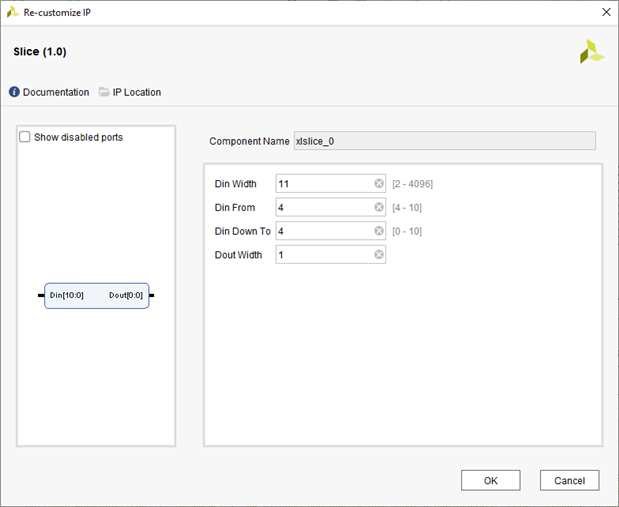
Slice slices a range of bits from the input. In this case I'm slicing 7 single bits from GPIO_O 4 thru to GPIO_O 10. These will provide the 7 inputs to my logic gates. With slice, you can specify the start and end range but you can only create a single output port. The first slice is shown here which will be connected to Input_A of the AND gate:
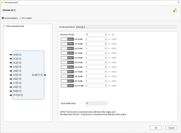
Concat concatenates multiple ports into a single port. With concat you can specify multiple input ports but only a single output port. Vivado will complain if the width of the ports between the ZYNQ7 Processing System IP and the Concat IP don't match, and unfortunately unlike slice, you cannot specify the begin and end for the range of bits you want to use on that port. As the note in the dialog declares, In0 is always connected to the LSB of the output port, so by increasing the number of input ports from the 4 required up to 11 is a workaround allowing you to connect inputs to specific output port bits. In this case it doesn't really matter, as I started my inputs at GPIO_I 0 thru GPIO_I 3 and then continued my outputs starting from GPIO_O 4.
There are another 53 bits of EMIO available so this design could easily be expanded to accommodate 16 switches, 16 LED's, 7-seg displays etc as found on the various trainer boards.
Some features of slice would be useful to have in concat and some features of concat would be useful to have in slice. A more generic on and off ramp block might help tidy things up and perhaps it make it more intuitive for those starting out, especially if they are mainly relying on the Block Design tool for connections.
In order to connect Slice and Concat IP blocks to the ZYNQ7 Processing System IP GPIO ports, the EMIO peripheral I/O pin first has to be enabled:
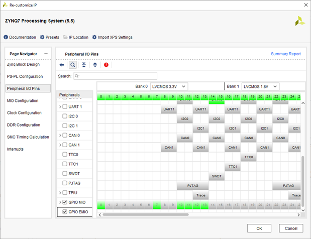
and the EMIO GPIO (Width) needs to be set. In this case to 11bits wide.
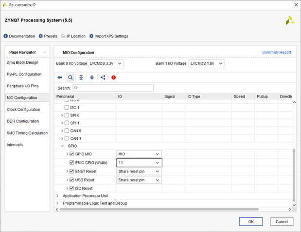
This adds the connection port to the block diagram and allows connections to the EMIO GPIO.
The 7 inputs of the four custom logic gate IP blocks are connected to the outputs of the 7 Slice IP blocks and the 4 outputs of the four custom logic IP blocks are connected to 4 of the 11 input ports of the Concat IP block. The resulting diagram looks like this:
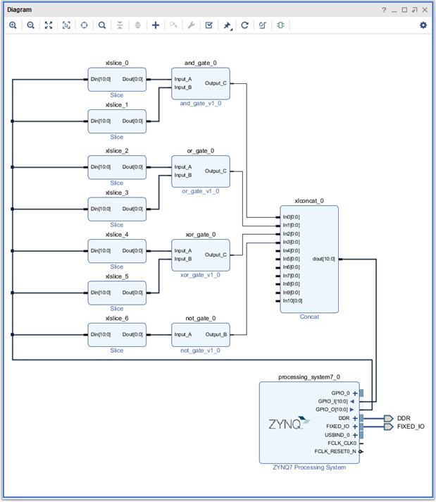
The GPIO_0 in the ZYNQ7 Processing system block relates to the newly enabled EMIO.
This completes the FPGA design and if it is all connected up correctly, then this will allow the input states of the four gates (LUTs) defined in the PL to be configured by Jupyter in the PS and the output states to be read using PS GPIO.
The final steps required in Vivado were to Validate Design, Create HDL Wrapper, Run Synthesis & Implementation, and Generate the Bitstream. The resulting files were copied over onto the PYNQ-Z2 dev board ready to be loaded into the PYNQ framework as a custom overlay.
Continuing the design in Jupyter Notebooks
Within the Jupyter environment a new notebook was created and within the IPython environment the newly created overlay was loaded.
from pynq import Overlay
ps_gpio_design = Overlay("./bitstream/mybitstream.bit")
Then we need to import the PYNQ GPIO module
from pynq import GPIO

The PS GPIO needs to be configured to set the direction of the ports. Here we set pins 0 to 3 as inputs. These connect to the Concat block via the GPIO_I port on the ZYNQ7 Processing System block
AND_output_C = GPIO(GPIO.get_gpio_pin(0), 'in')
OR_output_C  = GPIO(GPIO.get_gpio_pin(1), 'in')
XOR_output_C = GPIO(GPIO.get_gpio_pin(2), 'in')
NOT_output_B = GPIO(GPIO.get_gpio_pin(3), 'in')

Here we set pins 4 to 10 as outputs. These connect to the Slice blocks via the GPIO_O port on the ZYNQ7 Processing System block.
AND_input_A = GPIO(GPIO.get_gpio_pin(4), 'out')
AND_input_B = GPIO(GPIO.get_gpio_pin(5), 'out')
OR_input_A  = GPIO(GPIO.get_gpio_pin(6), 'out')
OR_input_B  = GPIO(GPIO.get_gpio_pin(7), 'out')
XOR_input_A = GPIO(GPIO.get_gpio_pin(8), 'out')
XOR_input_B = GPIO(GPIO.get_gpio_pin(9), 'out')
NOT_input_A = GPIO(GPIO.get_gpio_pin(10), 'out')

The PS GPIO is now all set up and we are finally able to test the function of each of the logic gates in the PL by setting their inputs and reading their output states.
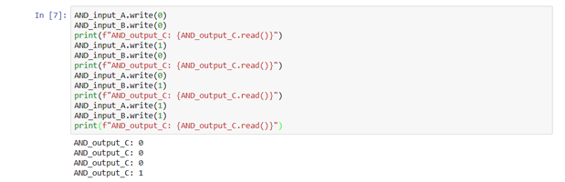
AND gate
AND_input_A.write(0)
AND_input_B.write(0)
print(f"AND_output_C: {AND_output_C.read()}")
AND_input_A.write(1)
AND_input_B.write(0)
print(f"AND_output_C: {AND_output_C.read()}")
AND_input_A.write(0)
AND_input_B.write(1)
print(f"AND_output_C: {AND_output_C.read()}")
AND_input_A.write(1)
AND_input_B.write(1)
print(f"AND_output_C: {AND_output_C.read()}")
OR gate
OR_input_A.write(0)
OR_input_B.write(0)
print(f"OR_output_C: {OR_output_C.read()}")
OR_input_A.write(1)
OR_input_B.write(0)
print(f"OR_output_C: {OR_output_C.read()}")
OR_input_A.write(0)
OR_input_B.write(1)
print(f"OR_output_C: {OR_output_C.read()}")
OR_input_A.write(1)
OR_input_B.write(1)
print(f"OR_output_C: {OR_output_C.read()}")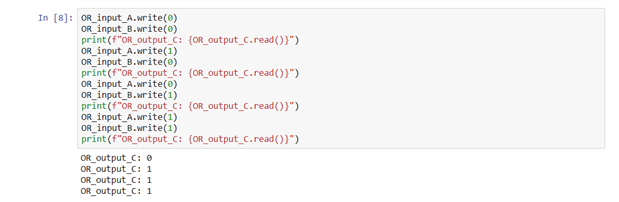
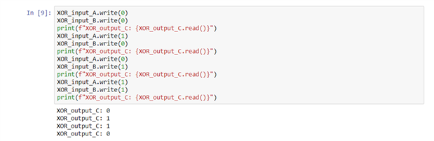
XOR gate
XOR_input_A.write(0)
XOR_input_B.write(0)
print(f"XOR_output_C: {XOR_output_C.read()}")
XOR_input_A.write(1)
XOR_input_B.write(0)
print(f"XOR_output_C: {XOR_output_C.read()}")
XOR_input_A.write(0)
XOR_input_B.write(1)
print(f"XOR_output_C: {XOR_output_C.read()}")
XOR_input_A.write(1)
XOR_input_B.write(1)
print(f"XOR_output_C: {XOR_output_C.read()}")
NOT gate
NOT_input_A.write(0)
print(f"NOT_output_B: {NOT_output_B.read()}")
NOT_input_A.write(1)
print(f"NOT_output_B: {NOT_output_B.read()}")

These logic gates all appear to be working as expected.
This completes the basic configuration and testing of EMIO GPIO on the PYNQ-Z2 dev board using the PYNQ framework.
The next step now is to look at how ipywidgets can be used to improve the user experience via interactive GUI objects within the Jupyter notebook environment.
Top Comments