


Introduction:
One of the standout feature of MAX32650 is its sigma-delta ADC with input and reference scaling option. Generally sigma-delta ADC is found in only application specific mcu and known for its accuracy. Another uncustomary feature of its ADC is its capability to monitor all the power supplies including VRTC. Apart from so many useful feature it is only lacking the ability to use external ADC voltage reference (Details: section 9 page 3 of MAX32650 Errata sheet: HERE). Here we will use the ADC of MAX32650 to monitor all the power supplies of MAX32650 as well as its ability to monitor voltages 5V signals with maximum limit of 9.7V at AIN0 and AIN1 even though according to MAX32650 datasheet the absolute maximum input voltage range for these inputs is 5.5V as shown in figure-1. Also we will learn how to modify the problem with MAX32650 ADC SDK library so the ADC example work properly without changing it. Even thought it is possible to make it work without modifying the SDK but it will require lots of changes in example code.

figure-1: Absolute maximum voltage rating of MAX32650 micro-controller
Details:
Before start testing the functionality of ADC lets look at the important details about ADC mentioned in USER guide. The block diagram of MAX32650 ADC shows all the important functionality. In the block diagram as shown in figure-2 the highlighted part doesn't exist/work. So its important to know before using the ADC and all of our calculation should be based on 1.22V internal reference.
figure-2: Block Diagram of MAX32650 micro-controller ADC - where ADC_CTRL > ref_sel doesn't exist/work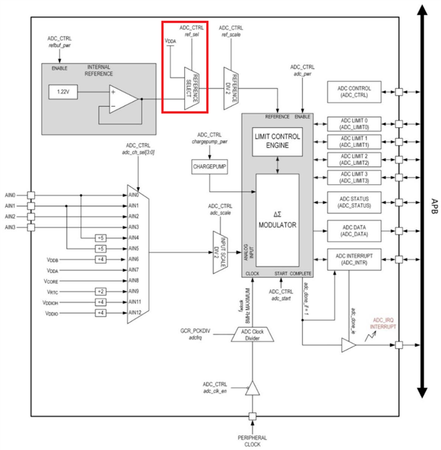
As the title suggest that it can be used to measure voltages well above the absolute maximum rating. So how is this possible when the equation 10-5 of MAX32650 (figure-3) while following the input/ref scale limitations of Table10-2 (figure-5) and also the ADC block diagram shows that AIN4=AIN0/5 and AIN5=AIN1/5? The answer is simple the data mentioned here is little confusing because user can assign the different input_scale and ref_scale to these with only limitation of maximum voltage limit will not be same as theoretical limit obtained from equation given below. During actual testing it is found that actual scaling for AIN4 and AIN5 is 5 and SDK ADC library is assigning constant 1 to input_scale irrespective user assigned value to it. In other word only the ref_scale for the AIN4 and AIN5 is user select able and input_scale value is ignored.
If using the default ADC library with ref_scale '0' the ADC_DATA equation given in figure 4 provides the correct ADC reading. According to this equation the maximum possible ADC reading should be 12.2V at 0x3FF but in reality the maximum achievable value is ~9.7V OR ~0X32F. If the Input voltage is increased further than ~9.7V the ADC voltage is dropped to ~6.28V OR 0x20F. So it means this the actual hardware limit instead of 5.5V when ref_scale is set to 0. The maximum limit ~5.5V is if and only if when ref_scale is set to 1. Apart from these significant errors in User guide there are several other typing mistakes in ADC section alone.
So we can find in ADC library that ADC input_scale for all the channel except first 4 is always 1. For channel 7 and channel 8, it is mentioned in the manual but not for rest of channels.
The ADC library code in ADC_StartConvert function that is setting the input_scale to '1' irrespective of user selected value.
// Finalize user-requested channel configuration
if (adc_scale || (channel > ADC_CH_3)) {
    ctrl_tmp |= MXC_F_ADC_CTRL_SCALE;
}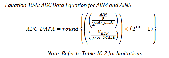
figure-3: ADC-DATA equation according to MAX32650 user guide
.
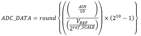
figure-4: ADC-DATA equation when ADC library is used (AIN/5 with constant input_scale of '1')
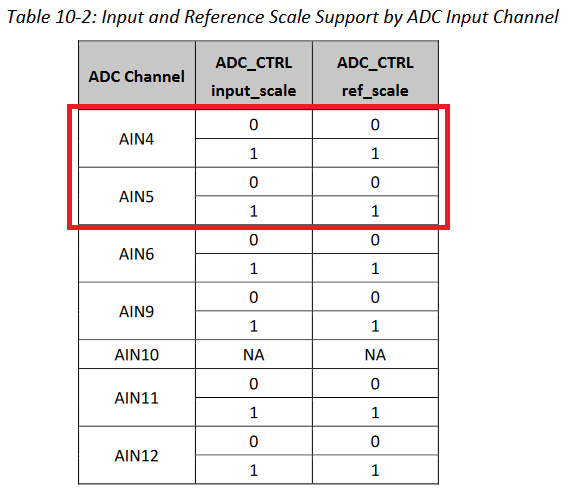
figure-5: AIN4 and AIN5 inputs scale limitation - MAX32650 micro-controller
Code:
The simplest solution of SDK ADC example problem of none detection of ADC_CH_1 upper and lower limits is to modify the problematic function of SDK ADC library. The main reason of this problem is the ADC_ClearFlags function of ADC library. In MAXIM provided library code this function is clearing all the interrupt flags irrespective of passed argument. To solve this issue the modified code is provided below.
void ADC_ClearFlags(uint32_t mask)
{
//   MXC_ADC->intr |= mask;                       // In Keil/IAR ARM pack
//   MXC_ADC->intr |= (mask & ADC_IF_MASK);       // In SDK for MAXIM IDE
     MXC_ADC->intr = MXC_ADC->intr & (0x0000001F | mask);    // Correct code to clear only the specified the interrupt flag
}
After replacing the problematic code line the MAX32650 SDK ADC example will work without any error with and without interrupts. And now it will print out the upper or lower limit detection message. The code given in ADC example is only useful when ADC limit is set for only one channel. the next method is useful for on single OR multi channel ADC limits.
Another way of achieving the same goal, with OR without modifying the ADC library function, of out of set ADC input limit detection for any channel is detection inside the ADC_IRQhandler function. With this method we can also find out which channel input is out of set limits especially when limit is set for multiple channels. (With interrupts ONLY)
Modified IRQ function for upper and lower limit detection for specific channel is given below.
/* **** Globals **** */
#ifdef USE_INTERRUPTS
    volatile unsigned int adc_done = 0;
    volatile unsigned int AN0_hi_limit = 0;
    volatile unsigned int AN0_lo_limit = 0;
    volatile unsigned int AN1_hi_limit = 0;
    volatile unsigned int AN1_lo_limit = 0;
#endif

#ifdef USE_INTERRUPTS
void ADC_IRQHandler(void)
{
        if(MXC_ADC->ctrl & ((ADC_CH_0 << MXC_F_ADC_CTRL_CH_SEL_POS) & MXC_F_ADC_CTRL_CH_SEL)){     // Check if current selected channel is AIN0 or not
            if (ADC_GetFlags() & MXC_F_ADC_INTR_HI_LIMIT_IF) {
                AN0_hi_limit=1;
            }
            if (ADC_GetFlags() & MXC_F_ADC_INTR_LO_LIMIT_IF) {
                AN0_lo_limit=1;
            }
            ADC_ClearFlags(MXC_F_ADC_INTR_HI_LIMIT_IF | MXC_F_ADC_INTR_LO_LIMIT_IF);
        }

        if(MXC_ADC->ctrl & ((ADC_CH_1 << MXC_F_ADC_CTRL_CH_SEL_POS) & MXC_F_ADC_CTRL_CH_SEL)){     // Check if current selected channel is AIN1 or not
            if (ADC_GetFlags() & MXC_F_ADC_INTR_HI_LIMIT_IF) {
                AN1_hi_limit=1;
            }
            if (ADC_GetFlags() & MXC_F_ADC_INTR_LO_LIMIT_IF) {
                AN1_lo_limit=1;
            }
            ADC_ClearFlags(MXC_F_ADC_INTR_HI_LIMIT_IF | MXC_F_ADC_INTR_LO_LIMIT_IF);
        }

        ADC_ClearFlags(MXC_F_ADC_INTR_DONE_IF);
    /* Signal bottom half that data is ready */
    adc_done = 1;

    return;
}
#endif
Code to set both upper and lower limit detection for AIN0 and AIN1.
/* Set up LIMIT0 to monitor high and low trip points for AIN0 */
ADC_SetLimit(ADC_LIMIT_0, ADC_CH_0, 1, 0x25, 1, 0x300);
/* Set up LIMIT1 to monitor high and low trip points for AIN1 */
ADC_SetLimit(ADC_LIMIT_1, ADC_CH_1, 1, 0x25, 1, 0x300);
The code to read the up to 9.5V (maximum ~9.7V) signal at AIN0 and AIN1 is given below. By following the scal limitation table the ref_scale value should be 1 for both of these channels. but for the experimentation only it is set to 0.
/* Convert channel 4 : input scale value is used */
#ifdef USE_INTERRUPTS
     adc_done = 0;
     ADC_StartConvert(ADC_CH_0_DIV_5, 0, 0);
     while (!adc_done);
#else
     ADC_StartConvert(ADC_CH_0_DIV_5, 0, 0);
#endif
     overflow[0] = (ADC_GetData(&adc_val[0]) == E_OVERFLOW ? 1 : 0);

/* Convert channel 5 : input scale value is used*/
#ifdef USE_INTERRUPTS
     adc_done = 0;
     ADC_StartConvert(ADC_CH_1_DIV_5, 0, 0);
     while (!adc_done);
#else
     ADC_StartConvert(ADC_CH_1_DIV_5, 0, 0);
#endif
     overflow[1] = (ADC_GetData(&adc_val[1]) == E_OVERFLOW ? 1 : 0);
The code to display the AIN0 and AIN1 is
uint8_t fmtstr[40];
uint16_t adc_val[2];
unsigned int overflow[2];

snprintf((char *)fmtstr, 40, "4: 0x%04x%s = %.2fV 5: 0x%04x%s = %.2fV",
         adc_val[0], overflow[1] ? "*" : " ", ((double)adc_val[0]/1023.0)*10.0*1.22,          // (ADC_DATA/(2^N-1)) x (Vref/2^ref_scale) x VIN_scale
         adc_val[1], overflow[1] ? "*" : " ", ((double)adc_val[1]/1023.0)*10.0*1.22);
printf("%s\n\n",fmtstr);
When ref_scale of '1' is used for the above channels then to obtain the right voltage, replace the 1.22 reference voltage multiplier with 0.61 in the above code.
Monitoring all the power supplies:
We can monitor all the power supplies internally without using any external ADC input. In here again the Input_scale has no effect on the output power measuring channels. And it seems like always at '1' or if doesn't has any effect on the signal then all the input signal dividers should be multiplied with 2 like ANI4 and ANI5 and table shown in figure-5 is incorrect.
In ADC library the only the first 10 channels are defined so user can either directly put the int value 11 and 12 in ADC_StartConvert function to measure VDDIO and VDDIOH voltages OR modify the MAX32650 ADC channels macros and enum to add these two channels in its library.
OPTIONAL: Add the following line in at the beginning of MAX32650 SDK ADC library header file adc.h
// Macros to select ADC channels
#define MXC_V_ADC_CTRL_ADC_CHSEL_AIN0                       ((uint32_t)(0x00000000UL))
#define MXC_V_ADC_CTRL_ADC_CHSEL_AIN1                       ((uint32_t)(0x00000001UL))
#define MXC_V_ADC_CTRL_ADC_CHSEL_AIN2                       ((uint32_t)(0x00000002UL))
#define MXC_V_ADC_CTRL_ADC_CHSEL_AIN3                       ((uint32_t)(0x00000003UL))
#define MXC_V_ADC_CTRL_ADC_CHSEL_AIN0_DIV_5                 ((uint32_t)(0x00000004UL))
#define MXC_V_ADC_CTRL_ADC_CHSEL_AIN1_DIV_5                 ((uint32_t)(0x00000005UL))
#define MXC_V_ADC_CTRL_ADC_CHSEL_VDDB_DIV_4                 ((uint32_t)(0x00000006UL))
#define MXC_V_ADC_CTRL_ADC_CHSEL_VDD18                      ((uint32_t)(0x00000007UL))
#define MXC_V_ADC_CTRL_ADC_CHSEL_VDD12                      ((uint32_t)(0x00000008UL))
#define MXC_V_ADC_CTRL_ADC_CHSEL_VRTC_DIV_2                 ((uint32_t)(0x00000009UL))
#define MXC_V_ADC_CTRL_ADC_CHSEL_TMON                       ((uint32_t)(0x0000000AUL))
#define MXC_V_ADC_CTRL_ADC_CHSEL_VDDIO_DIV_4                ((uint32_t)(0x0000000BUL))
#define MXC_V_ADC_CTRL_ADC_CHSEL_VDDIOH_DIV_4               ((uint32_t)(0x0000000CUL))


/**
  *    Enumeration type for the ADC Input Channels
  */
typedef enum {
    ADC_CH_0            = MXC_V_ADC_CTRL_ADC_CHSEL_AIN0,                    // Select Channel 0
    ADC_CH_1            = MXC_V_ADC_CTRL_ADC_CHSEL_AIN1,                    // Select Channel 1
    ADC_CH_2            = MXC_V_ADC_CTRL_ADC_CHSEL_AIN2,                    // Select Channel 2
    ADC_CH_3            = MXC_V_ADC_CTRL_ADC_CHSEL_AIN3,                    // Select Channel 3
    ADC_CH_0_DIV_5      = MXC_V_ADC_CTRL_ADC_CHSEL_AIN0_DIV_5,        // Channel 0 divided by 5
    ADC_CH_1_DIV_5      = MXC_V_ADC_CTRL_ADC_CHSEL_AIN1_DIV_5 ,        // Channel 1 divided by 5
    ADC_CH_VDDB_DIV_4   = MXC_V_ADC_CTRL_ADC_CHSEL_VDDB_DIV_4,        // VDDB divided by 4
    ADC_CH_VDD18        = MXC_V_ADC_CTRL_ADC_CHSEL_VDD18,                    // VDD18 input select
    ADC_CH_VDD12        = MXC_V_ADC_CTRL_ADC_CHSEL_VDD12,                    // VDD12 input select
    ADC_CH_VRTC_DIV_2   = MXC_V_ADC_CTRL_ADC_CHSEL_VRTC_DIV_2,        // VRTC divided by 2
    ADC_CH_TMON         = MXC_V_ADC_CTRL_ADC_CHSEL_TMON,                    // TMON input select
    ADC_CH_VDDIO_DIV_4  = MXC_V_ADC_CTRL_ADC_CHSEL_VDDIO_DIV_4,        // VDDIO divided by 4 input select
    ADC_CH_VDDIOH_DIV_4 = MXC_V_ADC_CTRL_ADC_CHSEL_VDDIOH_DIV_4,    // VDDIOH divided by 4 input select
} mxc_adc_chsel_t;
The code to read all the power supply internal channels of the ADC is;
/* Convert channel 6 = VDDB/8 OR VDDB/4 with input_scale is always '1' */
#ifdef USE_INTERRUPTS
     adc_done = 0;
     ADC_StartConvert(ADC_CH_VDDB_DIV_4, 0, 0);
     while (!adc_done);
#else
     ADC_StartConvert(ADC_CH_VDDB_DIV_4, 0, 0);
#endif
     overflow[0] = (ADC_GetData(&adc_val[0]) == E_OVERFLOW ? 1 : 0);

/* Convert channel 7 = VDDA and input_scale is always '1' */
#ifdef USE_INTERRUPTS
     adc_done = 0;
     ADC_StartConvert(ADC_CH_VDD18, 1, 0);
     while (!adc_done);
#else
     ADC_StartConvert(ADC_CH_VDD18, 1, 0);
#endif
     overflow[1] = (ADC_GetData(&adc_val[1]) == E_OVERFLOW ? 1 : 0);

/* Convert channel 8 = VCORE and input_scale is always '1' */
#ifdef USE_INTERRUPTS
     adc_done = 0;
     ADC_StartConvert(ADC_CH_VDD12, 1, 0);
     while (!adc_done);
#else
     ADC_StartConvert(ADC_CH_VDD12, 1, 0);
#endif
     overflow[2] = (ADC_GetData(&adc_val[2]) == E_OVERFLOW ? 1 : 0);

/* Convert channel 9 = VRTC/4 OR VRTC/2 with input_scale is always '1' */
#ifdef USE_INTERRUPTS
     adc_done = 0;
     ADC_StartConvert(ADC_CH_VRTC_DIV_2, 0, 0);
     while (!adc_done);
#else
     ADC_StartConvert(ADC_CH_VRTC_DIV_2, 0, 0);
#endif
     overflow[3] = (ADC_GetData(&adc_val[3]) == E_OVERFLOW ? 1 : 0);

/* Convert channel 10 = UNUSED*/
/*
#ifdef USE_INTERRUPTS
     adc_done = 0;
     ADC_StartConvert(ADC_CH_TMON, 0, 0);
     while (!adc_done);
#else
     ADC_StartConvert(ADC_CH_TMON, 0, 0);
#endif
*/

/* Convert channel 11 = VDDIO/8 OR VDDIO/4 with input_scale is always '1' */
#ifdef USE_INTERRUPTS
     adc_done = 0;
     ADC_StartConvert(ADC_CH_VDDIO_DIV_4, 0, 0);
     while (!adc_done);
#else
     ADC_StartConvert(ADC_CH_VDDIO_DIV_4, 0, 0);
#endif
     overflow[4] = (ADC_GetData(&adc_val[4]) == E_OVERFLOW ? 1 : 0);

/* Convert channel 12 = VDDIOH/8 OR VDDIOH/4 with input_scale is always '1' */
#ifdef USE_INTERRUPTS
     adc_done = 0;
     ADC_StartConvert(ADC_CH_VDDIOH_DIV_4, 0, 0);
     while (!adc_done);
#else
     ADC_StartConvert(ADC_CH_VDDIOH_DIV_4, 0, 0);
#endif
     overflow[5] = (ADC_GetData(&adc_val[5]) == E_OVERFLOW ? 1 : 0);

printf("VDDB: %.2f V%s | VDDA: %.2f V%s | VCORE: %.2f V%s | VRTC: %.2f V%s | VDDIO: %.2f V%s | VDDIOH: %.2f V%s\n\n",
     ((double)adc_val[0]/1023.0)*8.0*1.22, overflow[0] ? "*" : " ", ((double)adc_val[1]/1023.0)*2.0*1.22, overflow[1] ? "*" : " ",
     ((double)adc_val[2]/1023.0)*2.0*1.22, overflow[2] ? "*" : " ", ((double)adc_val[3]/1023.0)*4.0*1.22, overflow[3] ? "*" : " ",
     ((double)adc_val[4]/1023.0)*8.0*1.22, overflow[4] ? "*" : " ", ((double)adc_val[5]/1023.0)*8.0*1.22, overflow[5] ? "*" : " ");
In Keil the MAX32650 Ev-Kit ADC example need small setting change as shown below:
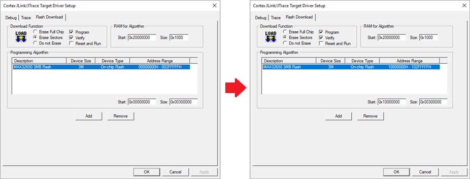
figure-6: Flash download setting for ADC example - MAX32650 micro-controller
Demo:
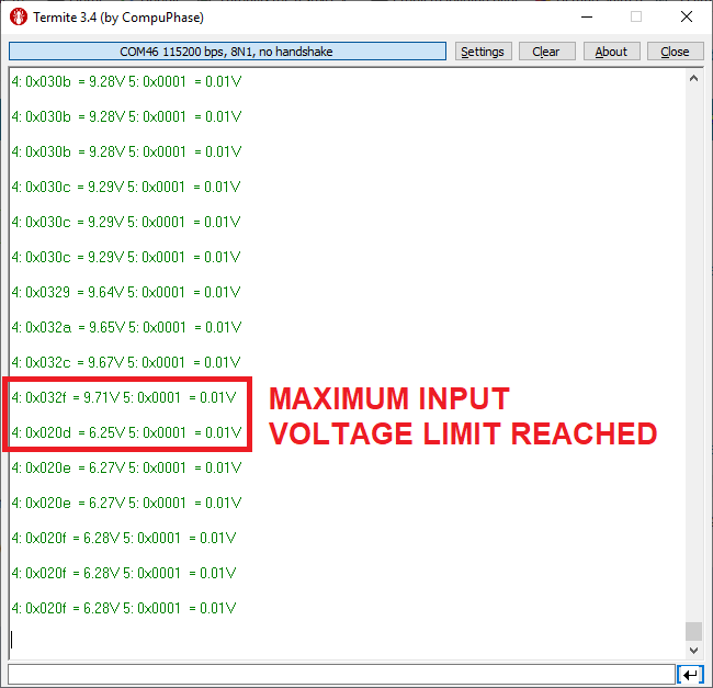
figure-X: Maximum ANI4 and ANI5 Analog inputs limit with unmodified ADC library (input_scale is 1) and ref_scale is 0 - MAX32650 micro-controller
.
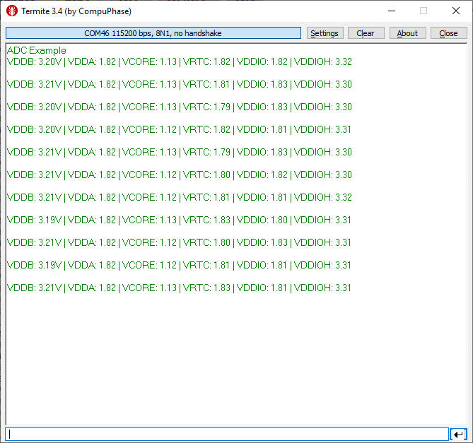
figure-X: All Analog inputs channels connected with Power supplies with unmodified ADC library (input_scale is 1) and ref_scale is 0 - MAX32650 micro-controller
For this experiment use the voltage supply with very limited current capabilities is used because when voltage is increased from ~9.7V, the voltage is dropped inside of ADC/micro-controller and excess current start flowing even though the voltage level at external AIN0/AIN1 pins remain at actual level. If the supply will be able to deliver lots of current then it can damage the micro-controller. SO APPLY ANY VOLTAGE ABOVE 9.5V AT YOUR OWN RISK.
Conclusion:
The ADC capabilities of this micro-controller definitely outshine from rest of the similar micro-controllers. We can also take the ADC to its hardware limit and measure analog values beyond ADC absolute maximum voltage limits mentioned in datasheet by not following the scale limitations mentioned in User Manual (use at your own risk because it can cause a permanent damage).
The ADC register configuration is way too simple and anyone can directly configure register without any problem. Even though there are some minor issue in ADC library but it can be avoided after little effort and some debugging. It will be better if all Maxim Integrated has provided a working MAX32650 ADC example same as mentioned in it description.
The ADC_ClearFlags function should be modified with function given below for proper operation and it should only clear the user selected interrupt flags instead of all the flags.
void ADC_ClearFlags(uint32_t mask)
{
//   MXC_ADC->intr |= mask;                       // In Keil/IAR ARM pack
//   MXC_ADC->intr |= (mask & ADC_IF_MASK);       // In SDK for MAXIM IDE
     MXC_ADC->intr = MXC_ADC->intr & (0x0000001F | mask);    // Correct code to clear only the specified the interrupt flag
}
Replace the ADC_StartConvert function input scale select code with this one to gain access of input_scale of all the ADC channels. But with gaining control of input_scale the user should also be aware about the fact that the maximum input signal limit will be the theoratical limit and he need to make sure that signals applied to these channels are below the physical ADC threshold level. And the actual code of library is only providing safety to ADC channel by keeping the voltage below the maximum hardware limit.
// Finalize user-requested channel configuration
//if (adc_scale || (channel > ADC_CH_3)) {     // ORIGINAL CODE
if (adc_scale) {                               // modified CODE
    ctrl_tmp |= MXC_F_ADC_CTRL_SCALE;
}
With unmodified ADC library the ref_scale should always be set to 1, except channel 7 and 8, to make sure that scales are according to limitation table 10-2 shown in figure-5.