


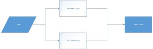
For the Digital Design (FPGA) aspect of the project we need the system to take inputs from the Mbed. Mostly it will be controlling Servos in a finite state machine, but when the system is in maintenance mode it needs to control the servos individually. This has lead me to come up with a quick block diagram of how the system should operate.
It will take the inputs via UART, the commands are then decoded (not shown) and sent to the relevant module. Both modules will output the to the same servo modules. This means that a buffer will probably be implemented on the maintenance mode outputs to force them high impedance during FSM operation. I am lucky in the fact that the FPGA board which we are provided with already has a UART Module on it, so I will not need to worry about writing one in verilog, i will just need to write the decoder.
As for the servos Drivers they are complete and have been tested via an oscilloscope. I would have tested with a servo attached, but it would appear that the IO Buffers on the board are busted and so the max output voltage is currently 66mV  and i will be talking to the lab technician about fixing/ replacing it. This is why the Signals bellow are so noisy, just due to a cheap scope and low voltages ( i am hopping)
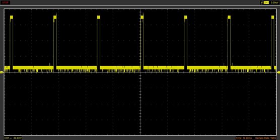

the images are not as clear as i would like and the software for my scope did not include the measurements of the period, and pulse width.
to Summarize the images, the first is a zero input to the servo module, which is producing a pulse width of approx 1ms.
the second is 255(Max) sent to the servo module, and is producing a pulse approx 2ms wide. So it works, apart from the low voltage, What i will probably try is an IO Port on a different buffer see if that fixes the issue. If you are interested in The Verilog Servo MOdule i have a write up here Verilog PWM
