element14 Community
element14 Community
    Register Log In
  • Site
  • Search
  • Log In Register
  • About Us
  • Community Hub
    Community Hub
    • What's New on element14
    • Feedback and Support
    • Benefits of Membership
    • Personal Blogs
    • Members Area
    • Achievement Levels
  • Learn
    Learn
    • Ask an Expert
    • eBooks
    • element14 presents
    • Learning Center
    • Tech Spotlight
    • STEM Academy
    • Webinars, Training and Events
    • Learning Groups
  • Technologies
    Technologies
    • 3D Printing
    • FPGA
    • Industrial Automation
    • Internet of Things
    • Power & Energy
    • Sensors
    • Technology Groups
  • Challenges & Projects
    Challenges & Projects
    • Design Challenges
    • element14 presents Projects
    • Project14
    • Arduino Projects
    • Raspberry Pi Projects
    • Project Groups
  • Products
    Products
    • Arduino
    • Avnet Boards Community
    • Dev Tools
    • Manufacturers
    • Multicomp Pro
    • Product Groups
    • Raspberry Pi
    • RoadTests & Reviews
  • Store
    Store
    • Visit Your Store
    • Choose another store...
      • Europe
      •  Austria (German)
      •  Belgium (Dutch, French)
      •  Bulgaria (Bulgarian)
      •  Czech Republic (Czech)
      •  Denmark (Danish)
      •  Estonia (Estonian)
      •  Finland (Finnish)
      •  France (French)
      •  Germany (German)
      •  Hungary (Hungarian)
      •  Ireland
      •  Israel
      •  Italy (Italian)
      •  Latvia (Latvian)
      •  
      •  Lithuania (Lithuanian)
      •  Netherlands (Dutch)
      •  Norway (Norwegian)
      •  Poland (Polish)
      •  Portugal (Portuguese)
      •  Romania (Romanian)
      •  Russia (Russian)
      •  Slovakia (Slovak)
      •  Slovenia (Slovenian)
      •  Spain (Spanish)
      •  Sweden (Swedish)
      •  Switzerland(German, French)
      •  Turkey (Turkish)
      •  United Kingdom
      • Asia Pacific
      •  Australia
      •  China
      •  Hong Kong
      •  India
      •  Korea (Korean)
      •  Malaysia
      •  New Zealand
      •  Philippines
      •  Singapore
      •  Taiwan
      •  Thailand (Thai)
      • Americas
      •  Brazil (Portuguese)
      •  Canada
      •  Mexico (Spanish)
      •  United States
      Can't find the country/region you're looking for? Visit our export site or find a local distributor.
  • Translate
  • Profile
  • Settings
Personal Blogs
  • Community Hub
  • More
Personal Blogs
Legacy Personal Blogs Transistors: Current Gain (Beta or hFE)
  • Blog
  • Documents
  • Mentions
  • Sub-Groups
  • Tags
  • More
  • Cancel
  • New
  • Share
  • More
  • Cancel
Group Actions
  • Group RSS
  • More
  • Cancel
Engagement
  • Author Author: jc2048
  • Date Created: 24 Mar 2017 1:07 PM Date Created
  • Views 3653 views
  • Likes 3 likes
  • Comments 1 comment
Related
Recommended

Transistors: Current Gain (Beta or hFE)

jc2048
jc2048
24 Mar 2017

Another 'Transistors' blog. I thought this one would be easy, but it turned out to be quite challenging and, in some

ways, a bit of a failure.


The current gain of a bipolar junction transistor (when the emitter is the common terminal between input and output)

is the ratio of collector current to base current. In some ways, it's the most fundamental parameter that the

transistor has, because our simplest conceptual model of the device is something that takes an input current and

produces an output current in proportion to it. Unfortunately, it's not a simple physical parameter - it depends on

other things and that's where all the complication sets in.


Here is what a multimeter shows for hFE for a particular 2N3904 transistor


image


That's nice and easy - a single number. But that's the DC current gain at a particular collector current, and for a

particular collector-emitter voltage, and at a particular temperature.


I decided to investigate the variation at different collector currents and for different C-E voltages.


Here's the circuit of my test set-up. This is the kind of design that accumulates as you're doing it, so some

aspects of it are a little odd and could probably be done better.


image


Quick talk-through. The top half is a constant-current source that defines the collector current of the device under

test. The opamp compares the voltage across the 47R resistor with the voltage that the 10k pot picks off the voltage

reference and drives the transistor so that they match. I wasn't worried about calibrating it as I had a meter

measuring the actual collector current - I just needed it to hold the current steady at the value I adjusted it to.

The odd arrangement with the two diodes is because the op-amp I used is a bipolar device and can't reach the rails

on either inputs or outputs - the diodes give the op-amp an extra volt and a bit to play with. The lower half of the

circuit might need a few moments thought to understand what it's doing. The op-amp drives the device under test so

that the collector sits at 0V. Once it has achieved that, and everything is stable, the base current is that

required to give the set collector current. The diode is just there to lift the voltage at the op-amp output so that

it doesn't have to get too close to the negative supply. Because the collector of the DUT (device under test) is now

held at 0V, the Vce value is whatever I set the negative rail PSU to. I could have used an ammeter to measure the

base current, but in practice I just measured the voltage across the 10k resistor and calculated the current.


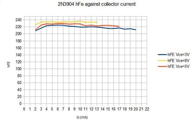
Here's the result of my tests on the same transistor that I measured with the meter


image


And here is how the hFE behaves for a fixed collector current and varying the Vce voltage.


image

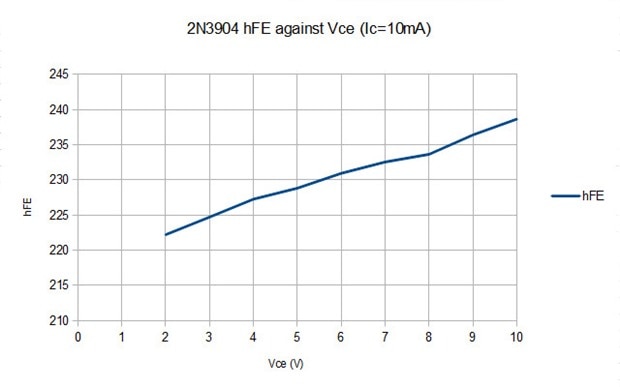
Unfortunately, I realised quite quickly that I had a major problem here. The transistor is small and has a low

thermal mass and, because the device self-heats and the hFE varies with temperature, I had readings that were moving

around even as I was trying to measure them. It was a particular problem at the higher Vce and collector current

values. The above graphs were the best I could do by letting the device cool, quickly moving to the required current

and voltage, and then taking an instant measurement. Even so, I don't manage the nice smooth curves that a

semiconductor manufacturer will show you on a datasheet. How do they do it? They use a pulse test where the

transistor is active for about 2% of the time. That would have been too complicated for me to do - I would have

needed a precision sample and hold to grab the readings - so I left things there.


If you want to get an idea of how the hFE varies with temperature, have a look at John Wiltrout's blog here (in the comments):


https://www.element14.com/community/people/jw0752/blog/2017/03/07/room-temperature-to-350-degree-c-hot-air-source-for-component-testing


Notes:


1) What I've been looking at here is the DC current gain in the common-emitter configuration, known as Beta or hFE.

The gain also varies with frequency and that is known as hfe.

2) Why beta rather than alpha? There is a parameter called alpha - it's the ratio of collector to emitter current.

[It's the gain when the base is the terminal that's common between input and ouput rather that the emitter.]

3) If you are designing with transistors, you just have to make the best of it (the variation of hFE). Often the

precise value doesn't matter and you just need to have a worst-case figure to work with. With amplifiers, where gain

accuracy is often important, feedback is normally used to shift the gain-setting on to accurate passive components

rather than the active devices.

4) I didn't come up with the form of the test circuit - the idea for servo-ing the base drive I stole from

"Transistor Circuit Design" by the engineering staff of Texas Instruments (published in 1963).

  • Sign in to reply

Top Comments

  • DAB
    DAB over 8 years ago +1
    Nice post. Every test provides valuable information. What you perceive as a failure is a very informative revelation about the need to understand what these parameters mean and how they were created. Your…
  • DAB
    DAB over 8 years ago

    Nice post.


    Every test provides valuable information.


    What you perceive as a failure is a very informative revelation about the need to understand what these parameters mean and how they were created.


    Your test confirms the basic numbers, but more importantly, it shows how delicate a circuit configuration can be to the environment in which it is used.


    On a personal note, you experiment confirms some of the issues I have been seeing as I apply my new atomic model to the structure of the semiconductor material.


    So keep up with these posts.  I for one find them very informative.


    Thanks

    DAB

    • Cancel
    • Vote Up +1 Vote Down
    • Sign in to reply
    • More
    • Cancel
element14 Community

element14 is the first online community specifically for engineers. Connect with your peers and get expert answers to your questions.

  • Members
  • Learn
  • Technologies
  • Challenges & Projects
  • Products
  • Store
  • About Us
  • Feedback & Support
  • FAQs
  • Terms of Use
  • Privacy Policy
  • Legal and Copyright Notices
  • Sitemap
  • Cookies

An Avnet Company © 2025 Premier Farnell Limited. All Rights Reserved.

Premier Farnell Ltd, registered in England and Wales (no 00876412), registered office: Farnell House, Forge Lane, Leeds LS12 2NE.

ICP 备案号 10220084.

Follow element14

  • X
  • Facebook
  • linkedin
  • YouTube