


EDITS: 14/6/19 - updated navigation link
27/6/19 - updated post for built power stage
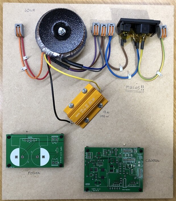
Prototyping Board
I'm waiting for new PCBs to come before cracking on with this but whilst I'm waiting I will work on the 4Duino interface and I created this prototyping board. The PCBs are the old ones (but don't change in size or appearance much). I've kapton taped the switch as well as used heatshrink tubing.
Building and Testing the Power Stage
There's been a bit of a hiatus as I've been busy at the museum and away in Berlin for a few days, however now it's back to it.
The new PCBs arrived very quickly - uploaded to JLCPCB on a Sunday, in my hands in the UK on the following Thursday. A quick check, and this time all seems ok. I'm building and testing the power stage first, so first off, cleaning the PCB and heatsink with IPA, then assembling the Bridge Rectifier on to its heatsink. My understanding for thermal paste is for it to 'fill any possible air gaps' and that the aim is to achieve a good case-to-heatsink connection and not to slather paste all over the place! So, a few dabs of paste:
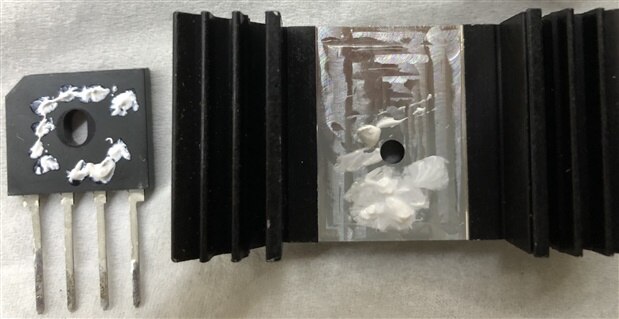
In the photo above you can see the reflective surface from the heatsink which looks a little like paste. This is because I hadn't paid enough attention to the data sheet for the heatsink and it has a spacing for a TO-220 package - clearly the bridge rectifier is much bigger. I had a colleague mill the spacing out to fit.
Spread the paste out:
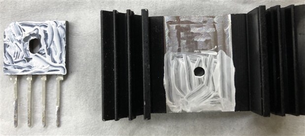
And assemble:
Screwing the BR to the heatsink has nicely spread the paste.
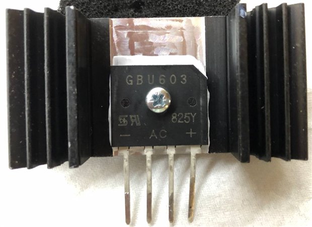
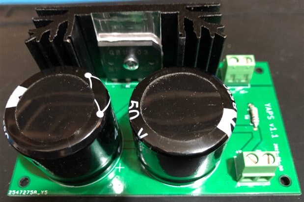
All the parts for the power stage were soldered onto the board, taking particular care that the capacitor polarity was correct! It's not a particularly complicated build but here it is in its glory:
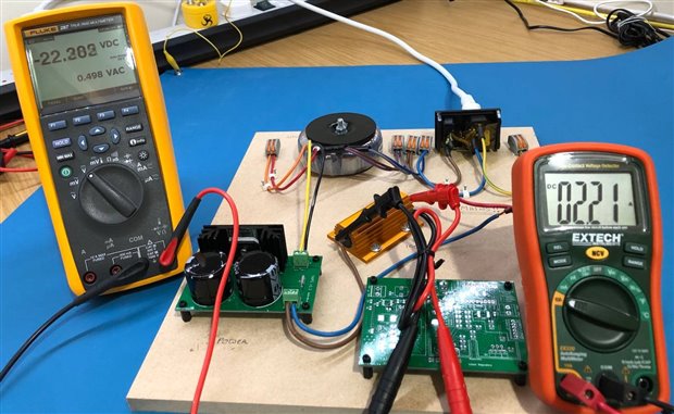
The moment of truth! I attached it to the prototyping board in the top picture, wired it up and, not without some trepidation I can tell you, turned it on. No fuse blown and 22.3Vdc and 2.21A is measured across the 10Ohm (5%) load (I realised afterwards I'd reverse connected the Fluke so it reads -ve, oh well.) That's pretty much in line with my expectations - my initial calculation was 2x9V out = 18VAC to the rectifier; 18V minus diode drop 2x0.9 = 16.2Vdc; 16.2 x sq.root 2 = 22.910Vdc. In my calculations post/spreadsheet, I used the values reported by LT Spice which were slightly higher at around 23.8Vdc so from a thermal perspective I'm slightly better off albeit by a smidgen - the main thing is that I'm not way off the wrong way!
I also measured the AC ripple, to the extent I can with the Fluke:
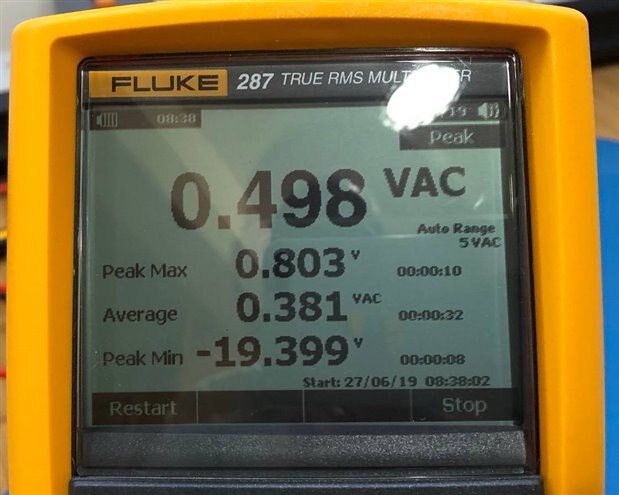
Here you can see the inrush of 19.399V, well within what I expected based on LTSpice, and a ripple peak of 0.803V. I'm going to assume that this is actually doubled for Pk-Pk (i.e. from -0.803V to 0.803V) which would give 1.6V Pk-Pk. Interestingly, the calculation for capacitors at an acceptable 1V implied a need for 30000uF capacitance for smoothing. If you read the notes associated with the calculation for Capacitors, you'll see that I made a specific choice to go with 2x4700uF given that the simulation of the design worked at this capacity - LTSpice reporting a 2V Pk-Pk at 3A.
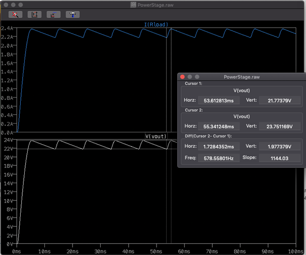
Here's the LTSpice view of things:
I don't have a brilliant scope yet, so I used the DSO Shell that I do have to measure this. Not ideal but it shows something not dissimilar:
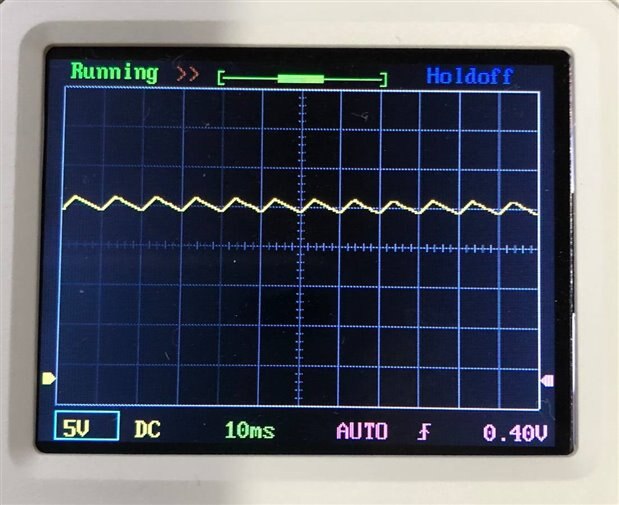
Given the scale I can use with this, it's showing around 2V Pk-Pk, probably a bit less, so I'd say that the Fluke, LTSpice and DSO are pretty much in agreement with each other and inline with the calculation I did. You won't believe how encouraging I find that!
Given that I've not blown anything up, that it seems to work in line with my calculations, and that I've not electrocuted myself I'm pretty pleased with the way that's gone. I really should invest in a scope though: I shall start to work on the wife  .
.
Top Comments