This is the third blog post in this series covering my road test evaluations of Advantech PCIE-1816 DAQ card and DAQNavi software. In this blog post I am planning to cover signal generation with the PCIE-1816 DAQ card and DAQNavi software.
In the previous two blogs I described how I installed the Advantech PCIE-1816 DAQ board in a computer and how I measured various signals with the 1816DAQ board and DAQNavi software. In this blog post I will show how I used the 1816DAQ board and the DAQNavi software to generate analog and digital signals.
I started by first setting up the voltage range of the analog outputs using the settings panel of the DAQNavi software program:
I have setup 0 – 10V voltage range on both channels, 10V reference, and 0V initial state. Next I opened the “PCIE1816_User_interface.pdf” document and I looked for instructions on how to connect the analog outputs. I like this document because it explains clearly and visually all I need to setup my test bench experiment:
I then connected an oscilloscope to the two analog outputs at pins 24 and 58. Here is a picture of my test bench setup:
I then setup sinusoidal signals at both channels using the DAQNavi waveform setup panel:
The sinusoidal signals were set to 1kHz frequency, 5V common mode, and 8V amplitude. I then clicked the “Start” button and I checked the generated waveforms on the oscilloscope:
The displayed waveforms show 8.6V amplitude, 5V common mode, and 0.998kHz frequency, close to the settings in the Advantech 1816DAQ board. Looking at the screen I see channel two sinusoid of 8V amplitude (based on 5V/div setting) and channel one sinusoid slightly higher amplitude, which is also measured with the built-in measurement functions.
Next I changed channel 1 of the Advantech 1816DAQ board to square wave signal, but I didn’t pay attention to the common mode, which remained to the 0V default. When I looked at the oscilloscope screen I noticed only 4V amplitude on the square wave signal instead of 8V:
I then realized my mistake, which was actually shown also in the graph window of the DAQNavi settings panel:
Notice the blue waveform chopped at 0V, so even though I setup 8V in the amplitude field the displayed waveform showed what signal will be generated. I then adjusted the common mode to 5V and the DAQNavi settings panel graph showed me the full 8V amplitude square wave:
The oscilloscope waveform matched the programmed one:
Next I changed the square wave into triangular waveform, also of 8V amplitude and 1kHz frequency:
The oscilloscope displayed these two waveforms as I was expected:
Following these experiments I focused on a single sinusoidal signal starting from 1kHz and gradually increasing the frequency until I reached the maximum that the DAQ board could generate. I have also set the voltage range to +/- 10V and the common mode to 0V.
I have tried to enter higher frequency values, but the DAQNavi panel always displayed the 30.303kHz, which is the maximum frequency that I could generate with this board. The waveform on the oscilloscope looked like an ideal sinusoid:
The measured amplitude and frequency came close to what I have programmed in the DAQNavi settings panel.
This waveform looked like a perfect sinusoid, but to further analyze the “quality” of this sinusoid I setup the oscilloscope to measure the FFT of this signal:
I was impressed of the quality of the generated sinusoidal signal. The fundamental frequency was measured as 30.3030kHz, which is exactly what I have programmed in the DAQNavi panel. There were no significant spurs and visually I could see that the phase noise is quite small compared to other oscillators that I have seen.
Next I switched to a square wave signal also of 30.303kHz frequency:
The oscilloscope displayed this waveform:
The measurements of frequency and amplitude were close to what I have programmed. The oscilloscope also measured the rise time and fall time. For 10.3V amplitude a rise time of 563.6ns (10%-90%) results in a slew rate of 14V/us, and similarly for falling edge 17V/us.
The FFT of this signal looked like an expected FFT of a square wave signal:
The fundamental is at 30.303kHz, exactly what I have programmed, and the harmonics are as expected for a square wave signal. I also wanted to check a triangular signal, and that FFT is shown in the picture below:
Next I generated digital signals. I first opened the “PCIE1816_User_interface.pdf” document, in which I looked for how to access the digital I/Os of the DAQ board:
So to generate digital signals I first had to configure the I/Os in output mode, and then I opened the digital output control panel in which I could toggle outputs by just clicking on corresponding buttons of the software panel. Here is the panel with all outputs set to 0V (logic “false” or low level):
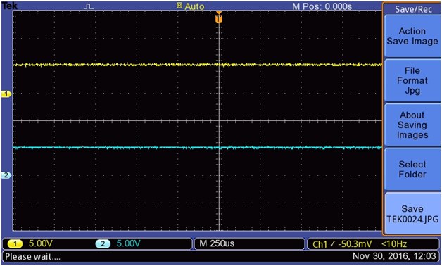
The oscilloscope showed 0V level on D0 and D1 outputs:
Next I toggled D0 in the DAQNavi panel:
And the oscilloscope showed D0 signal going to 5V (logic “true” or high level). Next I toggled D1 also, so both D0 and D1 were generating 5V, and I checked again the oscilloscope waveform:
I have checked various other combinations and all performed as expected.
Based on all these experiments described in this blog post I was very impressed of the quality of signals generated with the Advantech 1816 DAQ card and the easiness to setup the parameters of signals in DAQNavi software.
This concludes the third and last of the three blog posts I have planned for this review/evaluation. As a conclusion, I am impressed with the performance of this PCIE-1816 DAQ card and I am happy that I had the opportunity to road test it.
Best Wishes,
Cosmin


