element14 Community
element14 Community
    Register Log In
  • Site
  • Search
  • Log In Register
  • Community Hub
    Community Hub
    • What's New on element14
    • Feedback and Support
    • Benefits of Membership
    • Personal Blogs
    • Members Area
    • Achievement Levels
  • Learn
    Learn
    • Ask an Expert
    • eBooks
    • element14 presents
    • Learning Center
    • Tech Spotlight
    • STEM Academy
    • Webinars, Training and Events
    • Learning Groups
  • Technologies
    Technologies
    • 3D Printing
    • FPGA
    • Industrial Automation
    • Internet of Things
    • Power & Energy
    • Sensors
    • Technology Groups
  • Challenges & Projects
    Challenges & Projects
    • Design Challenges
    • element14 presents Projects
    • Project14
    • Arduino Projects
    • Raspberry Pi Projects
    • Project Groups
  • Products
    Products
    • Arduino
    • Avnet & Tria Boards Community
    • Dev Tools
    • Manufacturers
    • Multicomp Pro
    • Product Groups
    • Raspberry Pi
    • RoadTests & Reviews
  • About Us
  • Store
    Store
    • Visit Your Store
    • Choose another store...
      • Europe
      •  Austria (German)
      •  Belgium (Dutch, French)
      •  Bulgaria (Bulgarian)
      •  Czech Republic (Czech)
      •  Denmark (Danish)
      •  Estonia (Estonian)
      •  Finland (Finnish)
      •  France (French)
      •  Germany (German)
      •  Hungary (Hungarian)
      •  Ireland
      •  Israel
      •  Italy (Italian)
      •  Latvia (Latvian)
      •  
      •  Lithuania (Lithuanian)
      •  Netherlands (Dutch)
      •  Norway (Norwegian)
      •  Poland (Polish)
      •  Portugal (Portuguese)
      •  Romania (Romanian)
      •  Russia (Russian)
      •  Slovakia (Slovak)
      •  Slovenia (Slovenian)
      •  Spain (Spanish)
      •  Sweden (Swedish)
      •  Switzerland(German, French)
      •  Turkey (Turkish)
      •  United Kingdom
      • Asia Pacific
      •  Australia
      •  China
      •  Hong Kong
      •  India
      • Japan
      •  Korea (Korean)
      •  Malaysia
      •  New Zealand
      •  Philippines
      •  Singapore
      •  Taiwan
      •  Thailand (Thai)
      • Vietnam
      • Americas
      •  Brazil (Portuguese)
      •  Canada
      •  Mexico (Spanish)
      •  United States
      Can't find the country/region you're looking for? Visit our export site or find a local distributor.
  • Translate
  • Profile
  • Settings
Personal Blogs
  • Community Hub
  • More
Personal Blogs
Frank Milburn's Blog AIS Alarm - PCB Version 0.1 Fully Populated
  • Blog
  • Documents
  • Mentions
  • Sub-Groups
  • Tags
  • More
  • Cancel
  • New
  • Share
  • More
  • Cancel
Group Actions
  • Group RSS
  • More
  • Cancel
Engagement
  • Author Author: fmilburn
  • Date Created: 29 Jan 2018 10:03 PM Date Created
  • Views 759 views
  • Likes 4 likes
  • Comments 4 comments
  • daisy
  • smd
  • ais
  • pcb
  • msp430
Related
Recommended

AIS Alarm - PCB Version 0.1 Fully Populated

fmilburn
fmilburn
29 Jan 2018

Project Objective: Develop an open source AIS Alarm that alerts sailors that a new marine vessel with AIS is within range


Over the weekend the remaining parts arrived and I finished populating the board.  I found a few more problems and will document them here.  Normally I don't document problems unless they are somehow unique and instead give the final state but for this project I am going to publish warts and all.


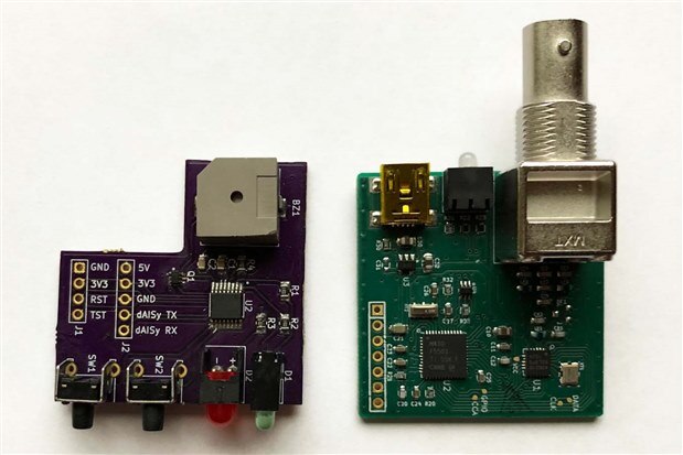
Here is the populated board next to a dAISy receiver.  The completed design will fold like a book over the dAISy with ribbon cable between the boards and slide into the aluminum case.

image

There are several problems which must be fixed along with a couple enhancements I intend to make in the next PCB:

  1. Interferences - One of the buttons is too close to the case and prevents easy sliding.
  2. Interferences - The space between the dAISy header and one of the LEDs on the alarm PCB is tight.
  3. Interferences - The buzzer and the dAISy LED interfere when in the case.
  4. Footprint - I used the wrong footprint on the large red LED (this really irritates me).
  5. Footprint - I used a standard footprint for the dual NPN MOSFET which made it hard to hand solder.


Regarding issues 1) through 3) I did not model in 3D but instead eyeballed everything and tried to measure by holding up a rule and working from data sheets.  I expected to make some adjustments but will end up making some big changes to accommodate the buzzer in the layout.


I was in a hurry when I submitted the board and issue 4. was easily preventable.  The pitch of the NPN MOSFET in issue 5. makes it difficult to solder anyway and I ended up having to clean up bridging on both sides.  A stencil and reflow oven would solve this, but I may just go with larger components in future designs.  LESSON LEARNED RELEARNED:  Haste makes waste (and delays).


In thinking through the issues it occurred to me that I can simplify the user interface and probably do not need the dual LED which is the source of one of the interferences.  Hopefully I will get out a revised PCB within the next week or so.


I ordered a couple of extra buzzers with the idea of testing to see how much difference there is between them.


In the meantime, this board is sufficient for me to continue development of the firmware.


Past Posts from this Project:

AIS Alarm

AIS Alarm - The Process

AIS Alarm - Prototype Hardware

AIS Alarm - Timers and GPIO

AIS Alarm - Prototype Code Outline

AIS Alarm - UART

AIS Alarm - First AIS Messages

AIS Alarm - First FRAM Storage

AIS Alarm - Debouncing Momentary Button Switches

AIS Alarm - FRAM Ring Buffer

AIS Alarm - Schematic

AIS Alarm - PCB Version 0.1

AIS Alarm - PCB Version 0.1 Arrived


References and Links:

WEGMATT LLC - dAISy AIS Receiver - low cost AIS receiver

Texas Instruments MSP430FR2xx FRAM Microcontrollers - Post No. 4

TI MSP430FR2111

Maximize the Sound from a Buzzer

  • Sign in to reply

Top Comments

  • fmilburn
    fmilburn over 8 years ago +2
    This photo shows the impact of the interferences: The slight *** is caused by the button being to close to the case. The interference between the buzzer and USB keeps the PCBs from sliding all the way…
  • genebren
    genebren over 8 years ago +2
    Frank, Looks like things are coming along nicely. Sure you were rushing and made a few mistakes. We have all done that. It is the desire to see your project come to life that prompts us towards a little…
  • three-phase
    three-phase over 8 years ago +1
    Thanks for the update, good to see the progress being made. Kind regards
  • fmilburn
    fmilburn over 8 years ago in reply to genebren

    Hi Gene,


    Thanks for comments... 


    It is a SOT363.  I had two problems - I used the default footprint in KiCad and the pads barely extend past the pins themselves on the package.  I used a toothpick to place solder paste on each pad but got too much.  I used a SMD rework station to flow the solder and there was bridging which I removed after several attempts with flux and an iron.  I believe it would have been easier if I had longer pads to pull the solder back on.  It always bothers me when I have to go back and reheat parts several times...


    Frank

    • Cancel
    • Vote Up 0 Vote Down
    • Sign in to reply
    • More
    • Cancel
  • genebren
    genebren over 8 years ago

    Frank,


    Looks like things are coming along nicely.  Sure you were rushing and made a few mistakes.  We have all done that.  It is the desire to see your project come to life that prompts us towards a little haste from time to time.

    On you dual MOSFETs, are those SOT563/SOT666/SSMINI6 packages?  Those things are almost impossible to solder.  I had to swap those out for some SOT363 parts which were still tricky, but way easier than the SOT666.


    Good luck on your layout reworks.

    Gene

    • Cancel
    • Vote Up +2 Vote Down
    • Sign in to reply
    • More
    • Cancel
  • fmilburn
    fmilburn over 8 years ago

    This photo shows the impact of the interferences:

    image

    The slight *** is caused by the button being to close to the case.  The interference between the buzzer and USB keeps the PCBs from sliding all the way without forcing.  It may not look like much but will require a new layout to fix.

    • Cancel
    • Vote Up +2 Vote Down
    • Sign in to reply
    • More
    • Cancel
  • three-phase
    three-phase over 8 years ago

    Thanks for the update, good to see the progress being made.


    Kind regards

    • Cancel
    • Vote Up +1 Vote Down
    • Sign in to reply
    • More
    • Cancel
element14 Community

element14 is the first online community specifically for engineers. Connect with your peers and get expert answers to your questions.

  • Members
  • Learn
  • Technologies
  • Challenges & Projects
  • Products
  • Store
  • About Us
  • Feedback & Support
  • FAQs
  • Terms of Use
  • Privacy Policy
  • Legal and Copyright Notices
  • Sitemap
  • Cookies

An Avnet Company © 2026 Premier Farnell Limited. All Rights Reserved.

Premier Farnell Ltd, registered in England and Wales (no 00876412), registered office: Farnell House, Forge Lane, Leeds LS12 2NE.

ICP 备案号 10220084.

Follow element14

  • X
  • Facebook
  • linkedin
  • YouTube