


When it comes to high-current requirements, the first thing that comes to my mind is testing MOSFETs. Ever since I received a batch of counterfeit MOSFETs, I’ve delved down into the rabbit-hole of testing MOSFETs under quasi-realistic application scenarios, chasing ever-more exotic parts that promise lower Rds(on) figures and compact surface-mount footprints. Unfortunately, only having a partially-functioning Rohde & Schwarz HMP4040 power supply, I could only really muster up 30A which isn’t quite enough to stress modern MOSFETs. The QPX750SP would change this … along with the latest contender of interest – the Infineon Source-Down MOSFETs.
MOSFET Test Preparations
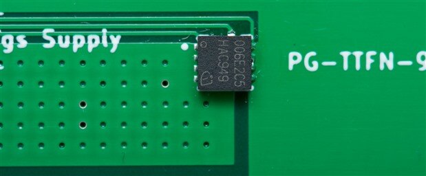
Before I could start cooking some MOSFETs, I had to do some homework. I wanted to compare the best TO-220 and PowerPAK SO-8 MOSFETs I had on hand to the Infineon Source-Down product. As a result, this would be a three-way battle between the NXP PSMN1R1-30PL (30V/1.1mΩ/120A), the Vishay SiRA50ADP-T1-RE3 (40V/0.86mΩ/219A) and the Infineon IQE006NE2LM5CGATMA1 (25V/0.65mΩ/298A) parts. It should be noted, there are better TO-220 and PowerPAK SO-8 parts out there, for example, the IRL50B209 (40V/1mΩ/195A) and SiR500DP-T1-RE3 (30V/0.39mΩ/350A), but I had neither to hand and didn’t feel it was necessarily worth ordering them as the TTFN-9 package (3.3mm x 3.3mm) offers an interesting size advantage over the SO-8 package (6.15mm x 5.15mm) and the centre-gate pin is a little different.
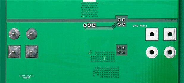
To actually conduct the test will require designing a test fixture in the form of a PCB. I previously designed a test PCB for my earlier tests using regular 1oz copper and 5.08mm terminal blocks for each 10A input from the HMP4040. This would not do at all. When dealing with such high currents, it seems nearly mandatory to use 2oz copper to reduce resistance and improve heat dissipation from the MOSFETs. Also, to convey 50A to and from the board itself would require 6mm2 wire to keep losses reasonable and reduce the potential for insulation damage, which also means that compatible terminal blocks were necessary. This necessitated 10.16mm blocks with two pairs of pins and designing my own footprint to accommodate. In the end, I designed a board specifically for this RoadTest and decided to make the most of the silk-screening. The manufacturing files for the board are attached to this post in case you are interested in manufacturing your own.


The design of the test fixture uses a board of about 100 x 100mm with most of the copper un-etched to offer heat-sinking capabilities. Thin traces are used for direct kelvin connections to measure Vds for each footprint, while the main current comes through up to three 10.16mm terminal blocks (in case higher currents are desired and other power supplies are used in parallel). The TO-220 footprint has been designed such that it can be “laid down” onto the board and offer better connectivity for the middle-pin and a path for heat to be dissipated through a plane on the other side of the board. In the case of the two SMD MOSFETs, a small island is used for the source connection which is made on the rear plane and plenty of plated-through-hole vias are used to ensure 50A can flow without generating excessive heat as I’m hoping they will act as a good thermal bridge to the copper on the rear. Almost by coincidence, both SMD MOSFETs have equal numbers of stitching vias. Four 3mm mounting holes are provided on each corner in case stand-offs are used or the board is repurposed for other uses in the future. Despite having several mounting footprints, I recommend having just one MOSFET installed on each board, so that failures and leakage from other MOSFETs in parallel will not affect measurements.
In the end, the shopping list added up to AU$171.68 to buy parts from element14 which I didn’t have on hand. Parts which I ended up using in this portion of the RoadTest included:
- Multicomp Pro PP001275 Red 6mm2 Wire (252810) x 22m – AU$56.41
- Camdenboss CTBP77VP/2CTBP77VP/2 Terminal Block (2668653) x 15 – AU$30.44
- Molex 19073-0123 Ring Tongue Terminal M8 (3222236) x 16 – AU$8.64
- Infineon IQE006NE2LM5CGATMA1 N-Channel MOSFET x 5 – AU$21.73
- 2oz 2-layer Copper PCB x 5 – AU$54.46
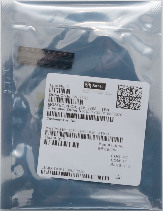
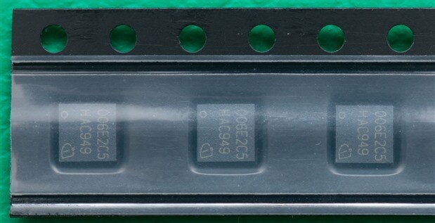
It did not take long for everything to arrive and the MOSFETs are absolutely tiny! I’ll have to continue using my “bodge” techniques to solder SMD components, but I was confident enough that it would be possible.
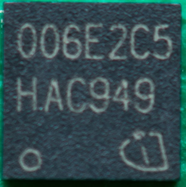
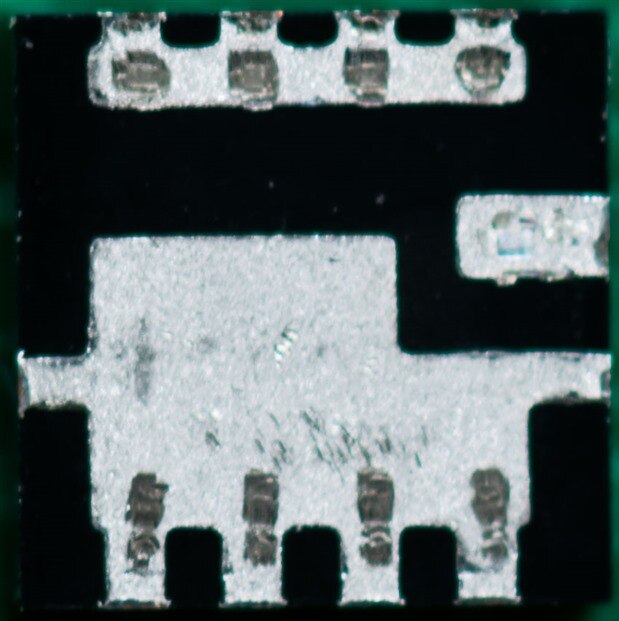
A close-up of the markings on the chip and the metal contacts on the package. Absolutely tiny, but that centre-gate contact could be nice for some applications and it keeps the gate and source having an equal number of pads.
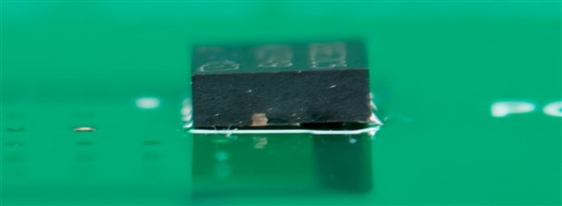
By using a tin-the-pads and hot-air-reflow-with-flux method, I was able to mount the package to the board although I am sure I have too much solder on one of the pads as the chip was not properly “sitting down” on the board. Regardless, I was confident that it was good enough to be serviceable.
Soldering the 10.16mm terminal blocks in place was a slight challenge for my Tenma combination rework station, but I got there in the end. The 2oz copper is very effective at wicking away the heat quickly!
In the end, I had my test candidates mounted with two terminal blocks on each, so I can call in my R&S HMP4040 with my newly designed parallel adapter for reinforcements in case 50A of torture is not enough for the MOSFETs. The crimp connector rings were “cut” to turn them into spades, so the QPX750SP would accept them.
Test Methodology
I decided that the testing would be a complex multi-instrument affair involving instruments from many vendors. The Aim-TTi QPX750SP would be responsible for providing the bulk of the drain-source current in constant current mode, while the Rohde & Schwarz HMP4040 would be called in if >50A is required. The gate would be driven by my Keysight E36103A configured to sweep from 16V down to 0V in 1mV steps. The voltage over the drain-source connection would be monitored by the Keithley 2450 SourceMeter acting as a high-precision voltmeter, although a decent digital multimeter could have sufficed.
This whole act would be co-ordinated by modifying my existing pyvisa script which runs the sweeps and computes the power dissipated in the MOSFET. If the power dissipated exceeds 3W, the test at that drain current is stopped. If the gate voltage is above 10V, then the test is terminated entirely. A cool-down time of 10 minutes is allowed between runs to avoid MOSFET overheating and provide a more consistent starting temperature. This script is executed by a Harting MICA Industrial Computer around the clock – even when I’m sleeping.
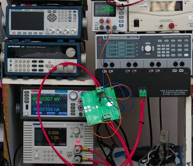
The collected data was used to draw comparisons by building Rds(on) versus Gate Voltage plots.
Results
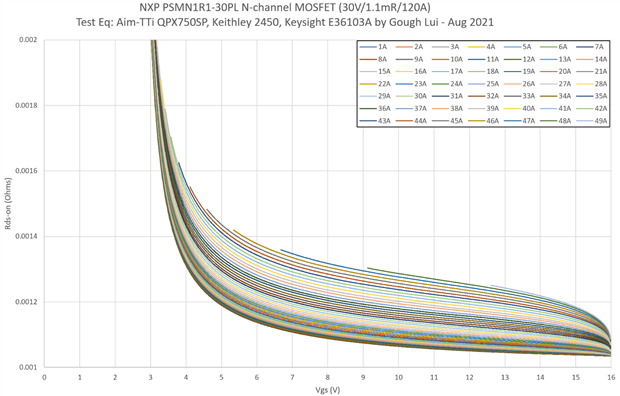
The first result is the NXP PSMN1R1-30PL TO-220 MOSFET which was able to make it to 49A before the test terminated completely. With a 10V drive, 48A could be handled on a PCB heatsink with the 3W power dissipation limit. At 5V drive, this could have been 45A. The Rds(on) at 10V shows a value of about 1.08mΩ at 1A, increasing to 1.25mΩ at 49A likely due to self-heating induced losses. The added current capability of the QPX750SP really helps to characterise things at higher current levels.

The second is the Vishay SiRA50ADP-T1-RE3 PowerPAK SO-8 MOSFET which also managed 49A before termination. That’s surprisingly similar! At 10V drive, it also managed 48A, while at 5V drive, it manages 43A. This seems to be in part due to a higher threshold voltage causing the curve to slope up sooner. The Rds(on) value at 10V was about 0.87mΩ at 1A, increasing to 1.28mΩ at 49A. This is higher than for the TO-220 which indicates potentially greater temperature sensitivity or poorer heatsinking, or both.
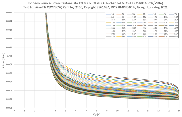
So, the million-dollar question, how did the Infineon IQE006NE2LM5CG fare? Quite well in a nutshell! I had to call in the reinforcements as the test didn’t terminate until 63A was passed through the tiny package. At 10V drive, it managed 62A and at 5V drive, it managed 58A which is pretty much a record. I can imagine you could run a scooter’s starter motor on that kind of current! The Rds(on) value at 10V ranged from 0.51mΩ at 1A, to 0.75mΩ at 62A. Of course, the 25V breakdown voltage is a little disappointing, but given the size, the performance is absolutely amazing. Perhaps this just means I should buy the SiR500DP-T1-RE3 (30V/0.39mΩ/350A) to see if the PowerPAK SO-8 can fight back!
Conclusion
High current capability is useful when it comes to characterising MOSFET capability under the expected application loads. Luckily for me, I was interested in the newly released Infineon Source-Down MOSFET series which offers a smaller package size with excellent Rds values and thermals, so I would compare how they fare with the best TO-220 and PowerPAK SO-8 MOSFETs I had on hand. For this test, my previous set-ups were relatively limited, so I had to make a few purchases and design a completely new PCB with 2oz copper to handle the high current.
Through a multi-instrument collaboration involving the Aim-TTi QPX750SP, Rohde & Schwarz HMP4040, Keysight E36103AE36103A, Keithley 2450 and Harting MICA Industrial Computer controlling the ensemble through a modified pyvisa script, I was able to automate the test procedure which involved sweeping the gate voltage while a constant current was being passed through the drain-source connection and recording the drain-source voltage at the package. The system automated a cool-down period on each run while also ensuring power dissipation would remain limited to 3W to avoid overheating of the MOSFETs which relied on PCB heatsinking. This allowed me to plot Rds(on) versus gate voltage plots which allowed for comparison of performance.
This process ran smoothly and the capability of the QPX750SP was instrumental in testing all MOSFETs. The tested NXP PSMN1R1-30PL and Vishay SiRA50ADP-T1-RE3 both reached 49A before hitting the power dissipation limit. The Infineon IQE006NE2LM5CGATMA1 proved to be a champion though, requiring a hefty 63A to reach the power dissipation limit. Of all the tested units, it offered the lowest Rds(on) even under load, however, it should be noted that there are better PowerPAK SO-8 MOSFETs so perhaps I should also give the SiR500DP-T1-RE3 a try as it claims an even more impressive 30V/0. 39mΩ/350A specification.
Throughout the test regime, the QPX750SP was reliably in-control via LAN and performed flawlessly. While I chose not to use its internal metering in favour of an SMU acting as a DMM to obtain higher accuracy in the computed plots, use of the sense terminals can certainly provide accurate readings down to 1mV resolution if that is sufficient.
---
This chapter is a part of the Aim-TTi QPX750SP 750W PowerFlex Programmable DC Power Supply RoadTest Review. More detailed chapters are linked from within the main review.