


In this exciting blog post, I will take apart the Digilent Analog Discovery Pro ADP3450 to see what it’s made of and how it’s been designed. This post will include a few nice photos of the internals along with a listing of some of the major parts that have been identified.
Teardown
The unit is easily opened by removing the six screws from the underside and then separating the lid. As the instrument would have been calibrated at the factory, opening the box is not advisable as it may cause the instrument to drift and become less accurate.
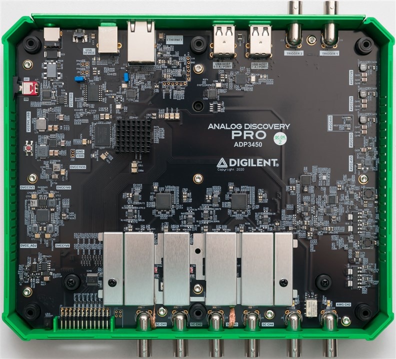
The instrument is quite light, so it is no surprise that the large black PCB we are greeted with is well spaced out with large empty areas. The silkscreen identifies the product with a copyright date of 2020, but also labels each group of components as to their purpose which can be very handy in case of modification or repair. The main IC under the heatsink is an Xilinx Zynq SoC, although I’m not going to remove the heatsink to find out. Let’s take a closer look at each of the well-labelled sections.
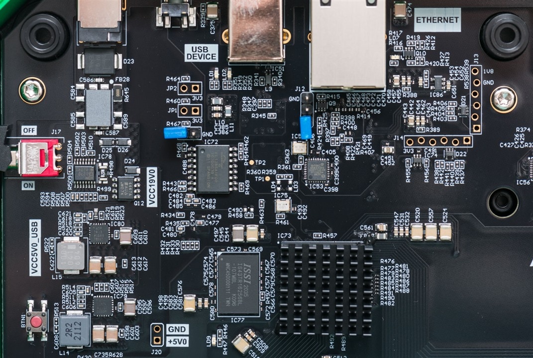
Starting in the top left, this area is responsible for power and interfacing. Key components include a Spansion FL128SAIF00 128Mbit Flash Memory which probably contains the bootloader and code for non-Linux modes, ISSI IS43TR16256BL-107MBL 4Gbit DDR3L 1866MHz C13 DRAM for a memory buffer, Microchip SMSC USB3320C Hi-Speed USB 2.0 Transciever for USB interfacing, Analog Devices ADM1270 Current-Limiting Controller and Vishay Si4447DY 40V P-Channel MOSFET as part of the power switching circuit. The VCC5V0_USB rail is provided by an Analog Devices ADP2443 Synchronous Step-Down DC-DC Regulator. It is nice to see the input is protected by a TVSS diode and filtered through a filter consisting of capacitors and a ferrite bead.
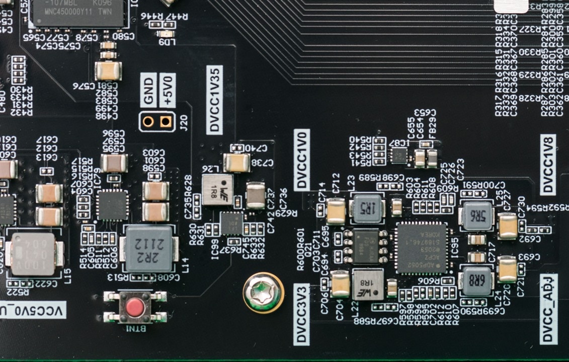
There are a number of other switching controllers which are not easily made out in the photo. It seems the DVCC_ADJ is sourced from the Analog Devices ADP5052 Integrated Power Solution with four high-performance buck regulators and an integrated LDO.
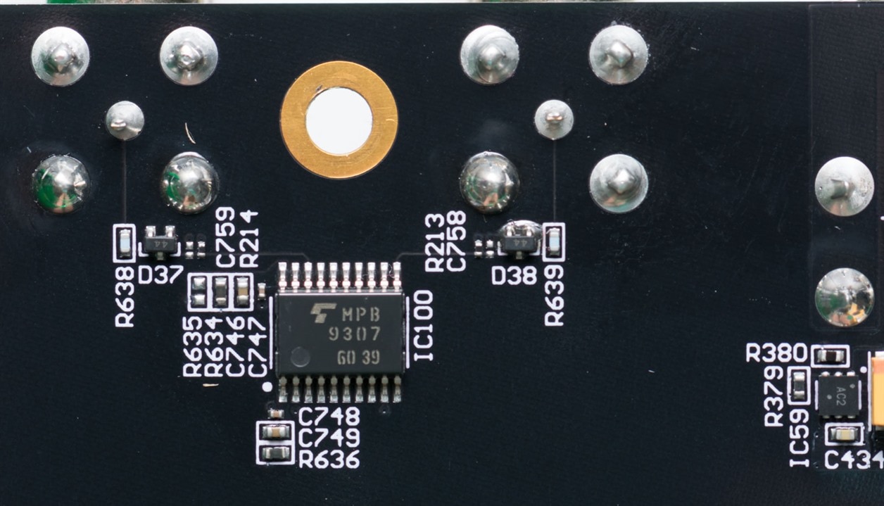
Perhaps some protection circuitry or another power regulator is situated on the underside of the board. Also seen is some digital logic circuitry including a Toshiba TC7MPB9307FK 8-bit driver.
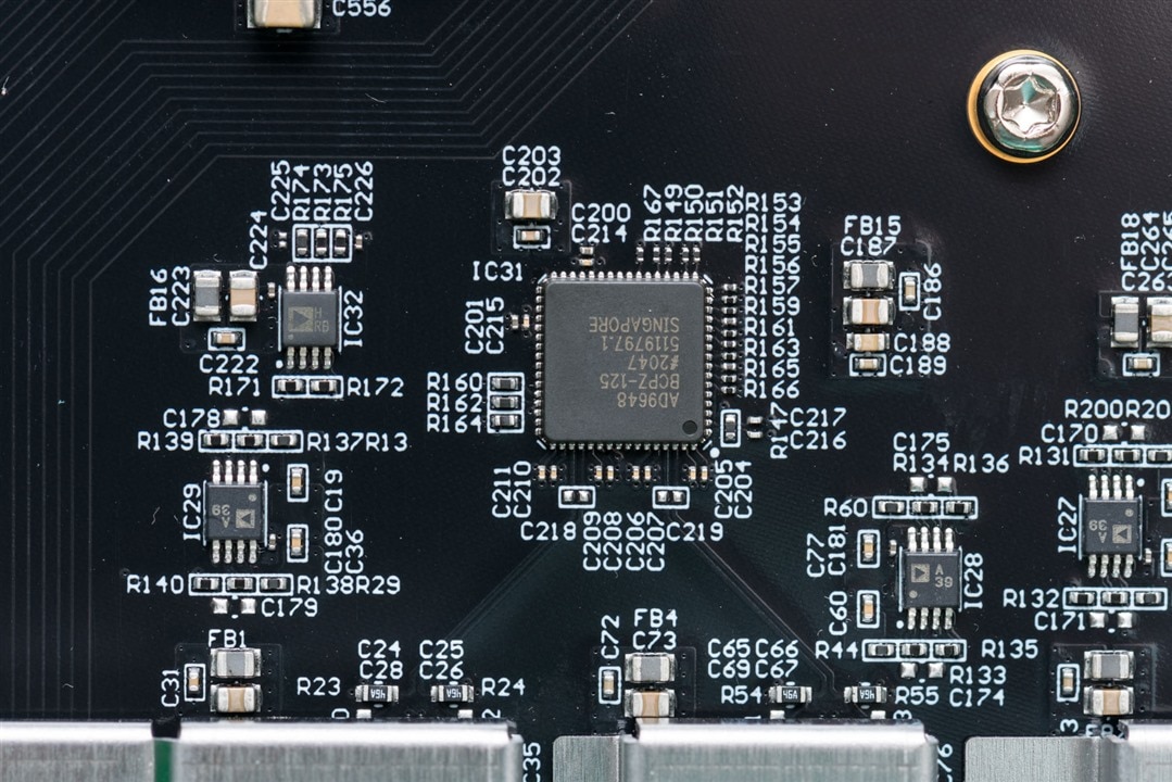
The oscilloscope channels follow a mostly symmetrical design, with an Analog Devices AD9648 dual-channel 14-bit 125 MSPS analog-to-digital converter taking care of each channel pair. This is complemented by a peppering of Analog Devices ADA4522 55V Ultralow Noise and ADA4841 Low Noise/Distortion Rail-to-Rail Op-Amps.
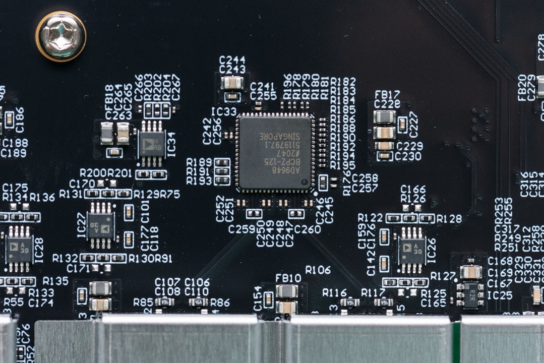
The other pair of channels in the ADP3450 are serviced by these components.
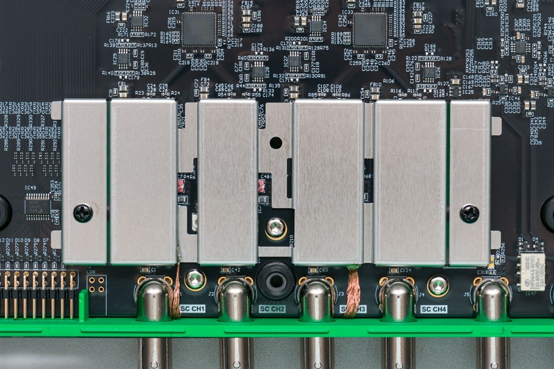
There are some front-end components which are hidden behind a metal shield – we will get to those later. However, this is the first time I’ve seen desoldering braid used in a commercial product to link the shield to a (presumably) ground point on the other side of the PCB.
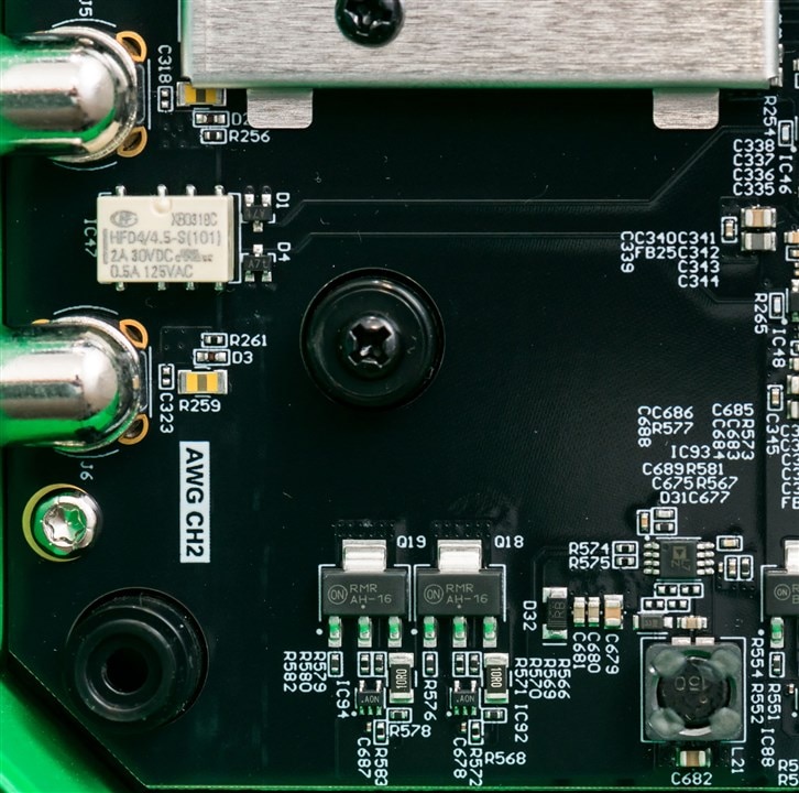
Now at the bottom-right of the top side of the PCB, near the wavegen outputs, there is a HongFa HFD4/4.5-S(101) relay. It seems each wavegen output is protected by a suspicious looking resistor – perhaps it is a polyfuse as well, or a fusible resistor. There is some DC-DC action as well, with an Analog Devices ADP1612ARMZ-R7 650kHz/1.3MHz PWM DC-DC Converter and a few On Semiconductor BCP53-16T1G PNP Transistors nearby.
The wavegen is driven by Analog Devices AD9717 14-bit low-power 125MSPS TxDACs and an AD5645R nanoDAC. Amplification seems to come from an Analog Devices AD8056 Low-Cost 300MHz Voltage Feedback Amplifier.
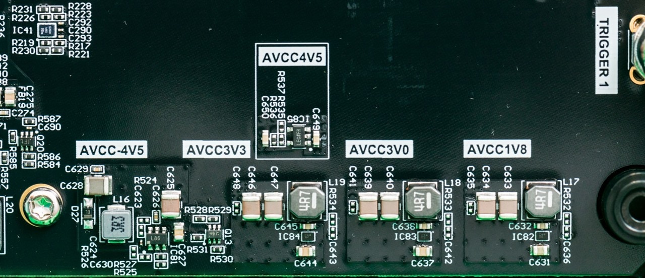
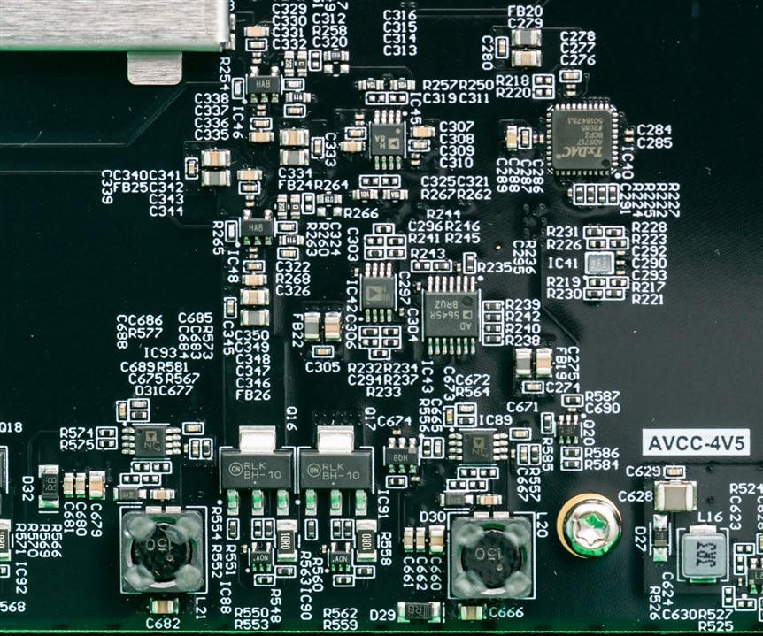
Other internal analog voltage rails are provided by switching converters as well, although I did not identify most parts in particular as SMD component markings can be quite cryptic. I do know that the AVCC-4V5 seems to be made via an Analog Devices ADP2301 1.2A/20V 1.4MHz Step-Down Regulator.
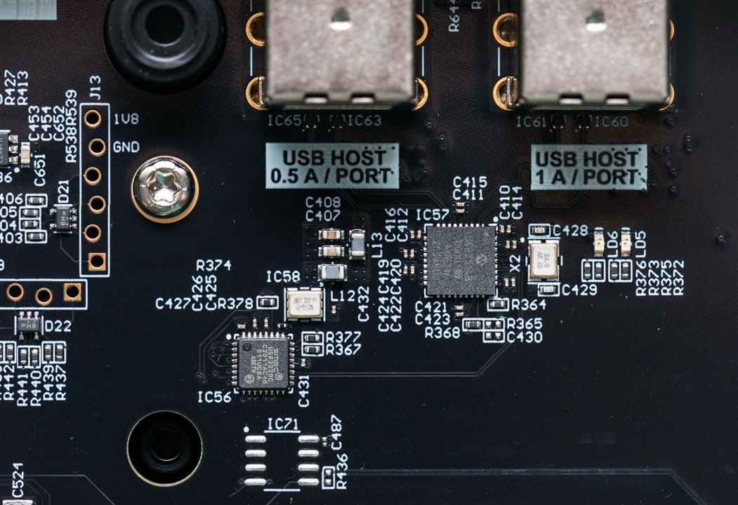
Back to the top of the port and near the USB ports, there is a Microchip USB2514B USB Hub Controller connected to a Microchip/SMSC USB3320C Hi-Speed USB 2.0 Transceiver.
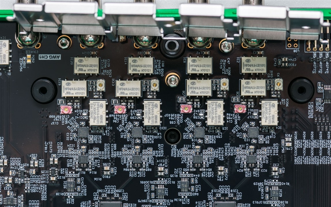
Peeking under the shield reveals a relay matrix with trimmer capacitors, most likely to allow for selecting bandwidth limiting, coupling and attenuation options. By all accounts, the three relays indicate the simplicity of the front-end design. The output feeds into an Analog Devices ADA4817 Low-Noise 1GHz FastFET Op-Amp and an unidentified IC marked 110 LCTC B939.
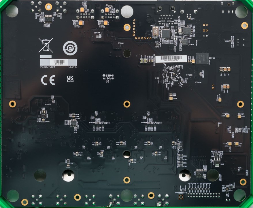
By comparison, the underside is relatively bare, although with a few rather important components. The board appears to be dated Week 13 of 2021 and has PB200-384 REV E written in the silkscreen.
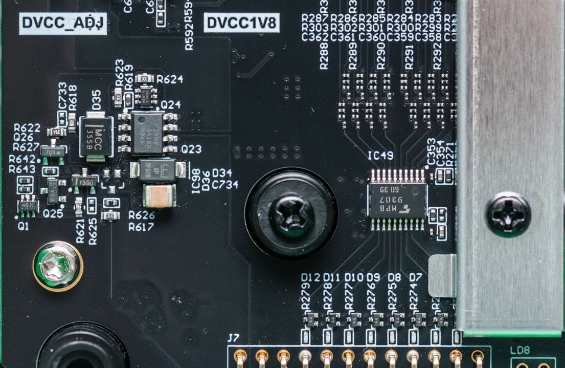
Another digital I/O driver can be seen, this one responsible for handling the trigger out ports.
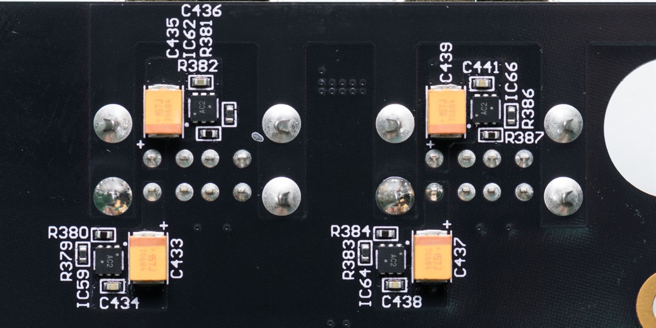
Near each USB port, there is some local bypass capacitors and a six-pin chip marked AC2 which probably provides some over-current protection or switching capabilities.
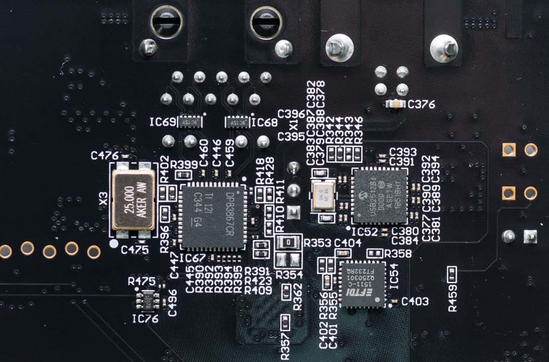
Near the USB host port, we see the remainder of the chips responsible for interfacing, including a Microchip USB2612B for which data is not available, but is likely to be some kind of hub, an FTDI FT232RQ which forms the 40MBit/s USB2.0 connection and a Texas Instruments DP83867CR Gigabit Ethernet PHY Transceiver for the Ethernet connection.
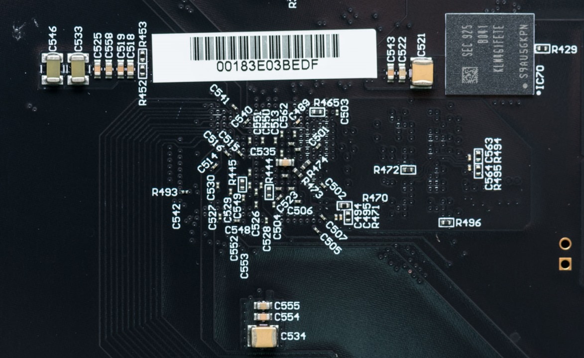
Behind the Zynq SoC is many vias and various small capacitors. To the side is a Samsung KLM4G1FETE 4GiB HS400 eMMC 5.1 which forms the main block device for Linux Mode.
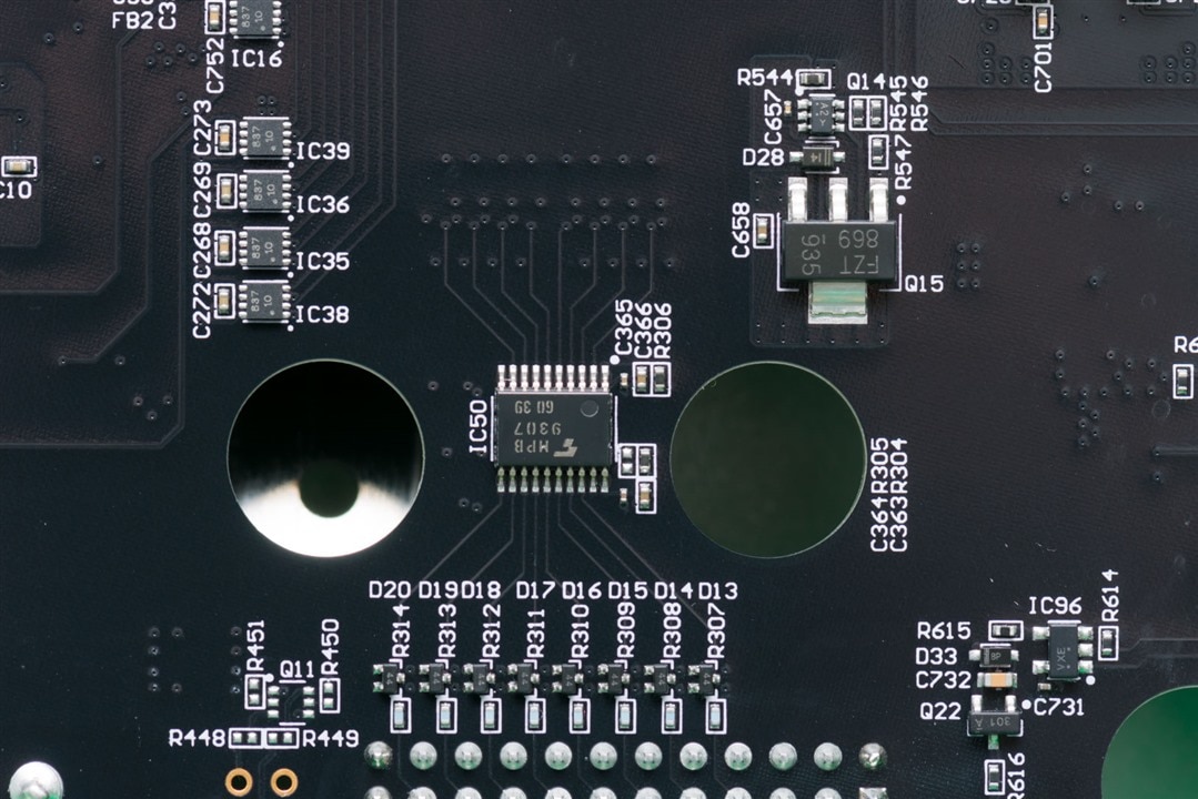
Another digital I/O driver, this one taking care of the “other” eight digital logic pins.
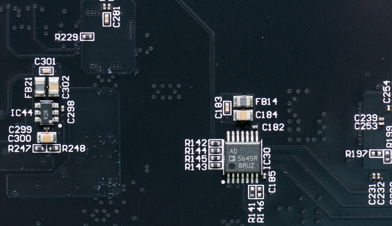
Finally, another AD5645R, likely for the second wavegen channel. The positioning on this side of the board may be to improve cross-talk characteristics and maintain a relatively symmetrical trace length/routing to improve channel-to-channel matching.
Conclusion
Looking inside the ADP3450 was an interesting exercise. The low weight implied that there would be quite a bit of empty space inside and this was borne out. Internally, the components predominantly came from Analog Devices which extends upon the tradition with the prior Analog Discovery and Analog Discovery 2 series boards, but this one does not seem to carry the co-branding. Regardless, the board was neatly constructed and well-labelled with the silkscreen which should aid future diagnosis, modification and repair if necessary. There are a number of buttons and jumper headers which are undocumented. Much of the ADP3450’s functionality is orchestrated by an Xilinx Zynq SoC which hides under a heatsink. The design has a surprising number of power rails, all derived by switch-mode conversion, occupying the outer edges of the board. Portions of the input matrix for the oscilloscope channels were shielded under a can, connected to ground via desoldering braid (which is an interesting approach). Pairs of oscilloscope channels share an AD9648 ADC. The wavegen output comes from an AD9717 TxDAC and AD5645R nanoDAC. The main boot device is a Spansion 128MBit Flash Memory, with an ISSI 4Gbit DDR3L memory buffer and a Samsung 4GiB eMMC for the main block device in Linux Mode. Various Microchip USB solutions are used alongside an FTDI FT232RQ which forms the USB device interface and a Texas Instruments DP83867CR Gigabit PHY Transceiver for the Ethernet interface. The design shows some special care taken to manage in-rush currents and power filtering.
---
This post is a part of the Digilent Analog Discovery Pro ADP3450 USB/Ethernet Mixed Signal Oscilloscope RoadTest Review.
-

DAB
-
Cancel
-
Vote Up
0
Vote Down
-
-
Sign in to reply
-
More
-
Cancel
Comment-

DAB
-
Cancel
-
Vote Up
0
Vote Down
-
-
Sign in to reply
-
More
-
Cancel
Children