


As one of the fortunate members to be selected to RoadTest the Keithley 2450 SMU, I delivered a review earlier this year with a significant caveat as a hardware issue stopped me from being able to perform some of the experiments I had initially planned. Following on from my series of follow-up posts comes this instalment which fittingly comes back full-circle to the experiment which led me to the discovery of the hardware issue in the first place.
Source-Measure Units, or SMUs for short, are often used to characterise semiconductor components during manufacture and testing. Their high accuracy, speed and ability to source voltage and current, both positive and negative, makes them ideal to run such tests. Something I’ve been wanting to do is to test the various types of n-channel MOSFETs that I have in my parts bins, but perhaps not in the way you might think.
I suppose there’s nothing too special about commercially available mass-produced components – after all, their performance is usually described in a datasheet and to great detail. For example, most datasheets have tens or more graphs showing various parameters including the all-important Rds vs Vgs and Ids vs Vgs amongst others. However, I was interested in some things that weren’t in the datasheets … some things perhaps a bit more destructive.
WARNING: Some MOSFETs were harmed in the production of this blog post, in the name of science, education and entertainment. Attempt these tests at your own risk.
User Experience - Keithley KickStart 2
While in my previous review, I had touched on using Keithley KickStart 2 in the trial mode, I didn’t have much time to explore all of the features available. After performing this round of experiments, I became much more acquainted with KickStart 2 and its features, some of which are quite handy.
Some of the features are not immediately obvious – for example, in my last posting on capacitor testing, I made the discovery that the graph axes could be changed and graphing versus time with voltage and current was a possibility simply by hovering over each axis and the legend to change the parameters. This increases the versatility of KickStart 2 to handle some non-I-V tasks using the I-V Characterizer module.
But then I also got into the documentation features. For example, each project can be named and saved, creating a .ksp (KickStart Project) file which contains various settings in XML along with a subfolder containing an .hdf5 (Hierarchical Data Format) file that bundles together the raw data from each run along with the settings that were used to obtain that data. Each run can be labelled with a description post-run completion and aborted runs are still saved. Tabled data view allows “hiding” data points in case there are specific outliers. The export functionality allows one-click batch exporting of all runs to .csv or .xlsx with .png graphs in selectable resolution, gridlines and light/dark palette.
In all, this makes running back-to-back experiments and saving results easy, even if you do intend to analyse them with third-party software, as the .ksp and .hdf5 files hold all the data and metadata together. The downside is that you will need KickStart 2 to export them into formats for import to your other software and it seems the naming of the files is defaulting to <app-name> <run> <time>, so I can’t seem to incorporate the run description into the filename.
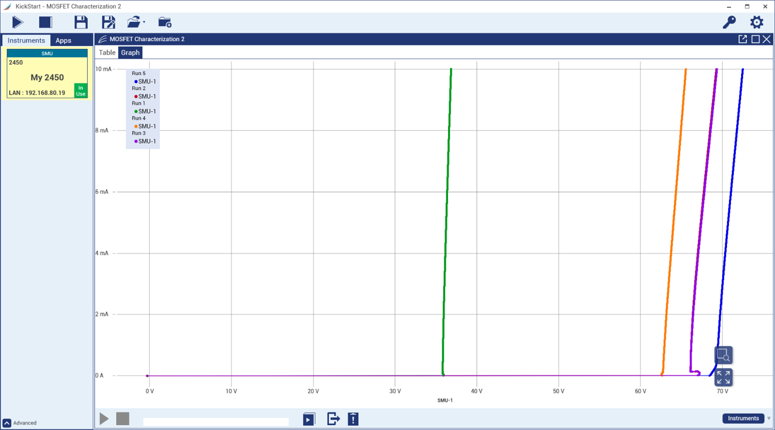
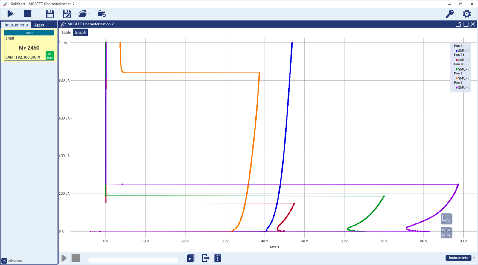
Another possibility once you have performed multiple runs within the same project is to select them to view them plotted together for visual comparison. This shows the later Vds Current Sweep and Vgs tests just directly plotted in KickStart 2.
While it is a software intended for no-hassle start-up use, the more I use it, the more I like it as I uncover its capability and flexibility. For example, if you just need a single voltage rather than an I-V sweep, there is the ability to run Voltage Bias or Current Bias mode. If you want to sweep through selected voltages or currents then there is a Voltage List Sweep and Current List Sweep option as well. If you’re doing a traditional Voltage Sweep or Current Sweep, it is possible to do a dual-sweep which allows for the value to be increased to maximum and decreased back to minimum. The addition of delay allows for waiting for the output to settle, while repeat allows for additional repetitions to be run automatically.
Some options seem rather innocuous at first but are perhaps key to the flexibility on offer – for example, the ability to disable auto-ranging and auto-zero altogether to prevent delays (important for devices which may not be at steady state – e.g. a device that is heating and shifting its operating characteristics during the test). It is possible to add power and resistance measurements, although it seems that the graphing doesn’t allow you to add a power curve to the plot after the run just by multiplying the measured voltage and current, which is a bit unfortunate. Other limitations with I-V Characterizer is the inability to perform measurements for a fixed period of time or at specific intervals – instead, the number of samples is specified up to 100,001 which seems to be a limitation of the size of the sample buffer type and size set by KickStart. But overall, I’d have to say that if I didn’t have KickStart, I’d have to spend quite a few hours developing my own a PC-hosted application that would remote control the 2450 and wouldn’t have such a polished user interface, or live with running TSP scripts on the 2450 to save data to a file and then manually analyse that afterward, so KickStart is a great convenience especially if you should so happen to own other equipment that is supported by KickStart making multi-instrument orchestration for certain tests a possibility.
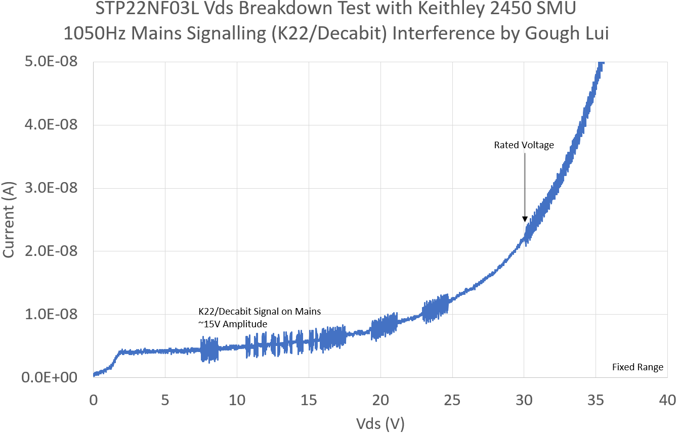
A little bonus finding was made when tracing out the I-V curve for this MOSFET using fixed ranges of 200V and 10mA (so as to ensure a regular sampling interval) and the mains ripple injection signalling (K22/Zellweger ~15V RMS at ~1050Hz non-phase-locked) was being used to command off-peak power. The resulting noise from the ripple injection caused about 5nA of current noise to appear in the measurements which clearly show the data being sent. According to the datasheet, the RMS noise <10Hz should be about 40nA sourcing in the 10mA range, so this seems to be within specifications although the noise may have also be the result of induction between the test leads and mains cables in the house as the signalling is not phase-locked with the mains frequency (thus the 1PLC setting would not have “averaged” it out perfectly on each sample).
Drain-Source Avalanche Breakdown Voltage
When using a MOSFET for switching tasks, one of the key parameters most designers will look at is the maximum Vds. This describes the maximum voltage that the MOSFET is capable of withstanding with the gate turned off at 0V. For most MOSFETs, exceeding the maximum Vds is a very bad thing as it could lead to spontaneous device destruction due to avalanche breakdown if the power dissipation is not carefully controlled. For MOSFETs that are avalanche rated, a certain avalanche energy is permissible, but generally speaking there may be some reliability cost to avalanche operation as it usually occurs first where the MOSFET is weakest, causing localised heating that may eventually lead to total destruction of the device. There are some instances though, where avalanche operation may occur and is designed into the system for cost reduction – for example, in power converters where ringing during switching may cause the maximum Vds to be exceeded for short intervals repetitively but with limited energy.
While Zener breakdown which happens in highly-doped semiconductor materials, avalanche breakdown happens in lightly-doped semiconductor materials and usually at higher voltages. It can happen very suddenly and is a form of runaway reaction where a strong electric field imparts enough force to free carriers in the transition region to collide with other bound electrons, creating even more free carriers.
This had me wondering – how “steep” is an avalanche breakdown? How much margin is there between the rated Vds and avalanche breakdown? Could we trigger such an avalanche breakdown using the SMU without destroying the MOSFET?
I-V Curves – Voltage Sweep
My first thought was to run a classic I-V curve on the MOSFET by sourcing voltage in steps between 0 to 200V with a current limit of 10mA set so that the dissipation in the MOSFET would not be enough to cause it to immediately catastrophically fail, although perhaps being a little “toasty”. This test took a relatively long time as I selected 10,001 steps for the voltage resolution and left the settings on auto-ranging which increased the test time, although many MOSFETs did reach the current limiter so the test could be aborted beforehand.
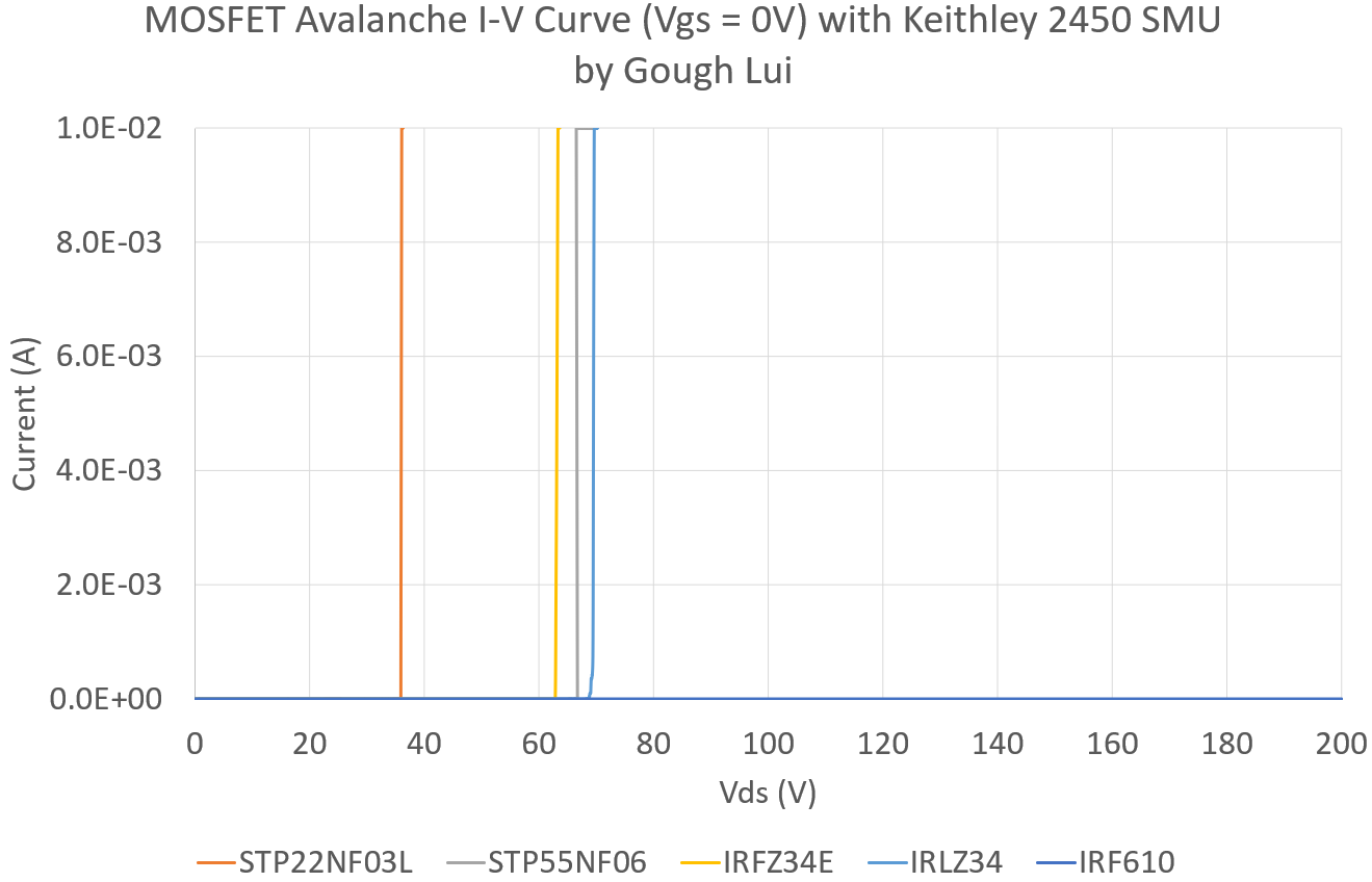
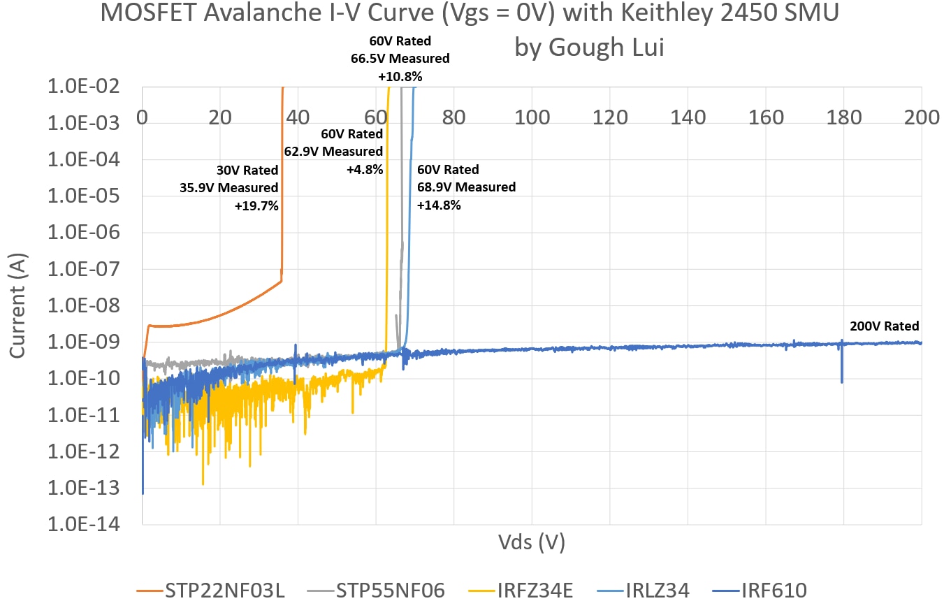
The results show the avalanche breakdown clearly for all MOSFETs except the IRF610 which has a Vgs rating of 200V (the set maximum limit of test voltage). In the linear graph, there’s not much detail visible in the avalanche at this scale, but the logarithmic scale graph shows some lower-level current detail. All tests are likely to be influenced by the test lead insulation resistance especially below the 0.5nA range. Interestingly, the STP22NF03L seems to be a bit “leaky” even when turned off.
In all cases, the measured values exceeded the rated values by anywhere from 4.8% to 19.7%, depending on the particular make of MOSFET.
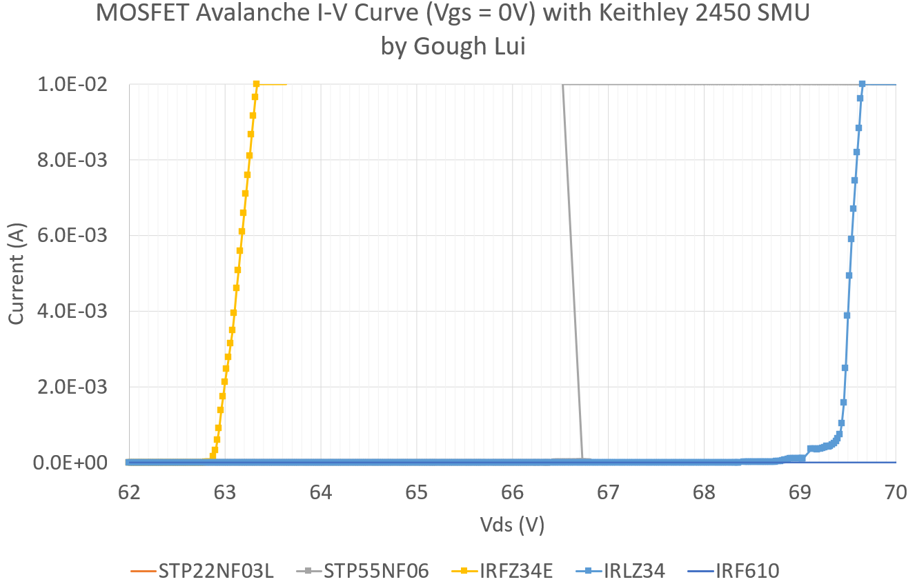
Zooming in to the 62-70V region, we can see the relatively limited resolution in the avalanche range due to the fixed size of voltage steps. In the case of the STP55NF06LSTP55NF06L, there were no datapoints during the avalanche range as the device “snapped” into conducting 10mA in-between two voltage steps and is hence stuck in constant current from there.
Obviously, while this achieves the aim of identifying the voltage level at which avalanche occurs for these MOSFETs without destroying them, it is relatively slow and still doesn’t provide much resolution in the avalanche region.
I-V Curves – Current Sweep
One of the advantages of the 2450 SMU is the ability to source current rather than voltage. This means we sweep current, rather than voltage, so we can immediately see what it takes to push a certain level of current through the MOSFET. In this case, I set the current limit to 10mA with just 1001 steps for a much faster test that should hopefully give me what I’m hoping to see – definition in the avalanche region.
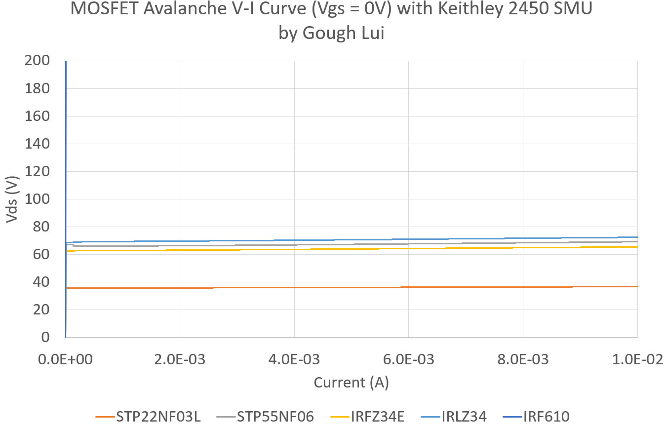
The axes in this case are reversed from the traditional I-V curve, in this case, plotted as V-I instead. This perhaps doesn’t look all that interesting, but zooming in provides a bit more definition.
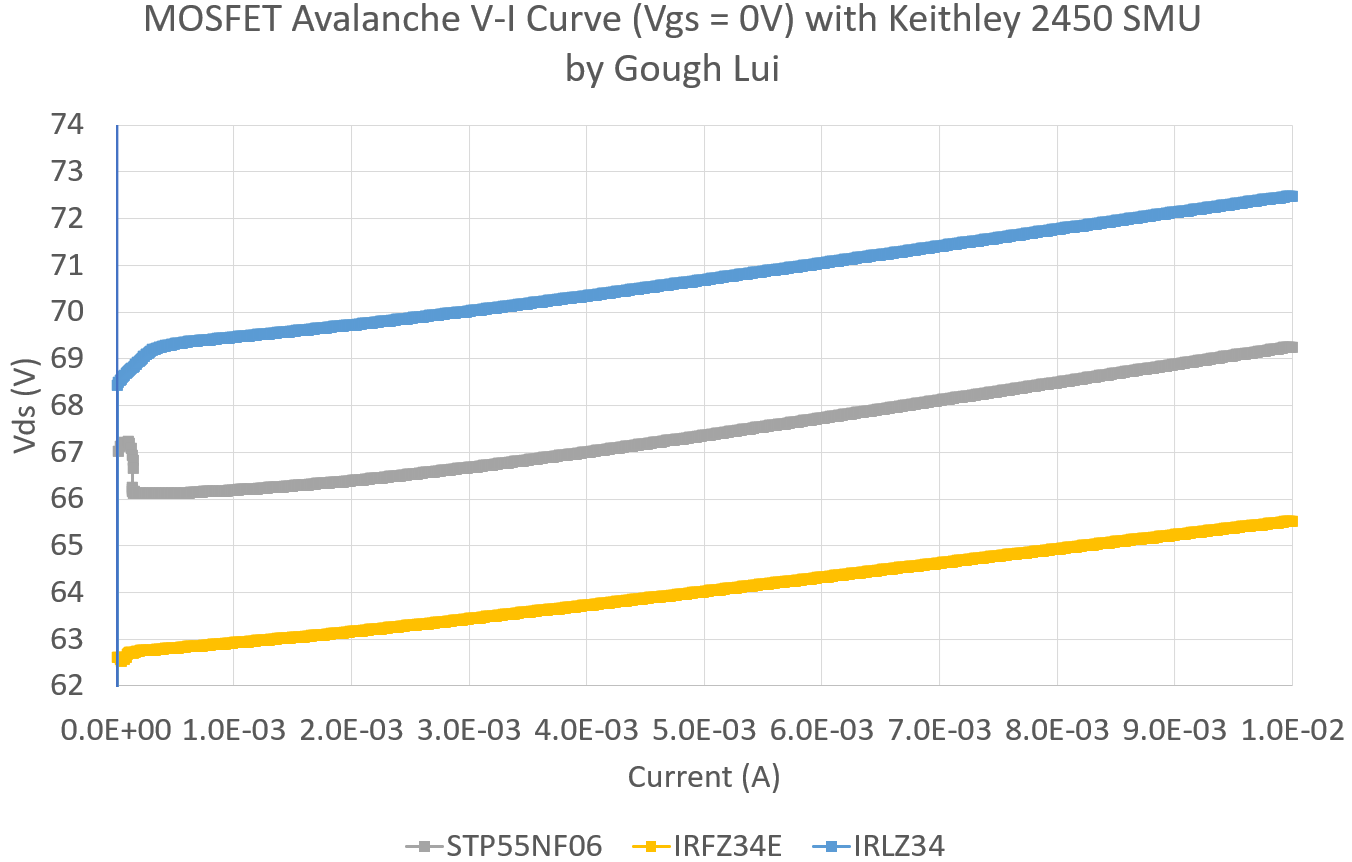
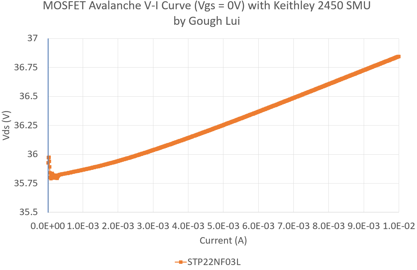
In the case of the MOSFETs which did suffer avalanche breakdown, we can see that from ~0 to 10mA, the avalanche breakdown spans about two to four volts and there is some instability at the initial point of breakdown.
Gate-Source Breakdown Voltage
In a MOSFET, the gate terminal controls the state of the channel through the field effect. The MOSFET is mainly a voltage-mode device, with the gate being a sort of “capacitor”, insulated from the channel with a thin layer of oxide. The geometry of the oxide can impact the sensitivity, reliability and performance of the MOSFET. This oxide layer generally is an insulator with a low leakage current, contributing to the efficiency of using MOSFETs over BJTs. However, the MOSFET can be broken down by overvoltage and this is one of the key reasons why MOSFETs are so ESD sensitive.
Most MOSFETs have absolute maximum Vgs ratings of around 10-20V, with lower ratings commonly observed for “logic level” drive MOSFETs. Again, I wondered how much voltage could a gate tolerate before it failed entirely and what would be the result. Instead of running an I-V curve sourcing voltage as before, I decided to start pumping current through the gate instead to get a “quick” answer, stepping the current at 1µA intervals with 1001 steps which is perhaps not the best way of going about it given the ordinary leakage is in the order of 100nA as I’d miss some of the lower-level results.

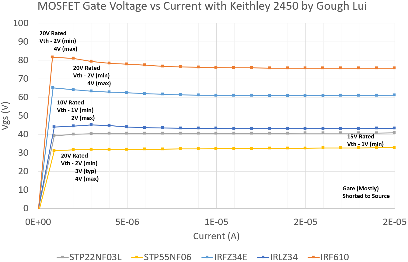
I suspect that pushing such current through the gate is basically setting a voltage that forces charges to tunnel through the oxide and any imperfections or weak spots within the oxide layer. Depending on the geometry, the behaviour of the MOSFET will differ. As I am not an expert in semiconductor device physics, the following interpretations will be based on my prima-facie assumptions, but on the whole, there didn’t seem to be any great correlation between Vgs rating nor Vgs(th) ratings with the points of failure or Vgs attained.
The STMicroelectronics StripFETs seemed to have lower Vgs voltages developed, but handled current up to 841µA before blowing through to a medium-resistance short to source in the case of the STP55NF06STP55NF06. The STP22NF03L managed the full 1mA current without failure, which was a surprise. The lower voltage I suspect indicates the presence of more leakage points within the oxide possibly reflecting a larger gate geometry, however, the lack of abrupt failure early in the test may indicate that the oxide was very homogenous so there was no weak spot to concentrate current flow and cause a thermal failure.
The Vishay Siliconix IRFZ34E and IRLZ34 are very much “related” devices, with the “L” device featuring a lower voltage threshold and lower Vgs as a result, but otherwise similar specifications. Indeed, both devices blew through their gate oxide at similar levels of 188µA and 150µA respectively which might reflect similarities in device geometries and oxide quality. The attained Vgs differed – in this case, the lower-level device had a Vgs that was about 18V lower than the higher level device, both higher than the STMicroelectronics devices.
The Samsung Electronics produced IRF610 oldest device in the bunch with a not-so-impressive Rds and intended for use with higher voltages (Vds = 200V) had an even higher Vgs, reaching above 75V while pushing current through. The oxide blew through at 250µA. In all cases of IRF failures, the oxide failure resulted in a much lower resistance short of the gate to source – usually <= 90 ohms.
As a result, it was interesting to see that there is a big variance – in the case of the STP55NF06LSTP55NF06L which is rated to 20V, it saw about 39V before it failed entirely. The IRF610 rated to 20V managed to reach 88V. While this test was the result of testing a single sample and you can’t depend on any MOSFET to exceed its datasheet rating, the margin seems to be highly dependent on the device design (e.g. geometry, materials, purity) and is very part-specific. The amount of current you need to blow the gate can be quite small - 150µA in the case of the IRLZ34, but the STP22NF03L proved to be the exception, tolerating even 1mA in this short-term test. But given the relatively low currents and voltages found in this test, it is clear that ESD definitely has the potential to destroy MOSFET gates.
Conclusion
This blog brings me full-circle to the experiments which first uncovered the hardware issue with my review Keithley 2450 SourceMeter unit. The completion of these experiments serves as proof that the RMA repair process was successful in addressing the original problems.
My adventures in testing MOSFETs for “destructive” parameters proved interesting, as it gave me an opportunity to further explore the capabilities of the Keithley KickStart 2 I-V Characterizer module and software in general. The more I used it, the more I liked it as I “discovered” features which make it easy to get going with experiments with sufficient flexibility to accommodate various needs. For example, the various modes available in the I-V Characterizer means that it is possible to perform non-I-V experiments as well (using Voltage/Current Bias modes) and custom steps (using Voltage/Current List modes) as well. Even settings which seem innocuous (e.g. auto-ranging/auto-zero) are provided and provide the ability to improve test speed or reduce test artifacts from auto-ranging delays. Being able to hide bad data points, label test runs with descriptions, reconfigure graph axes, add cursors, plot/compare multiple runs, save test settings/data in a single .ksp/.hdf5 project set and bulk-export to .csv/.xlsx/.png all proved very useful and time-saving compared to trying to develop your own software.
I did find several limitations, including the inability to set export filename based on test run description, to plot a power line based on multiplying voltage and current after a run has completed and to set time-based or interval-based acquisitions (especially for Voltage/Current Bias modes where this may be useful). On the whole, however, I think Keithley KickStart 2 is a very useful piece of software especially if you have multiple supported instruments where it would even allow orchestrating experiments across multiple devices.
The experiment found that all MOSFETs were able to provide some margin to the Vgs rating, ranging from 4.8% to 19.7% depending on the make of MOSFET. By using current-sourcing for another I-V test, it was possible to get finer detail within the avalanche breakdown region, where it was found that it occurs over a range of about two-to-four volts. The gate-source voltage breakdown tests proved destructive, as I set a current limit of 1mA, but it showed clear differences in results with STMicroelectronics parts having a lower Vgs voltage to achieve current leakage, but withstanding higher levels of leakage before blowing through the oxide and shorting the gate to source. The Vishay Siliconix IRLZ34 only managed 150µA of current flow before the oxide layer blew through. This clearly illustrates how MOSFET gates can easily be damaged by electrostatic discharge, however, also shows the allowable Vgs rating may have quite a bit of margin. No clear correlation between Vgs ratings and Vgs(th) ratings were seen with the final Vgs achieved or the amount of current taken to blow through the oxide layer – this is likely because of multiple causes of variation include device geometry and material quality. I’d count this as “curiosity satisfied!”
