element14 Community
element14 Community
    Register Log In
  • Site
  • Search
  • Log In Register
  • Community Hub
    Community Hub
    • What's New on element14
    • Feedback and Support
    • Benefits of Membership
    • Personal Blogs
    • Members Area
    • Achievement Levels
  • Learn
    Learn
    • Ask an Expert
    • eBooks
    • element14 presents
    • Learning Center
    • Tech Spotlight
    • STEM Academy
    • Webinars, Training and Events
    • Learning Groups
  • Technologies
    Technologies
    • 3D Printing
    • FPGA
    • Industrial Automation
    • Internet of Things
    • Power & Energy
    • Sensors
    • Technology Groups
  • Challenges & Projects
    Challenges & Projects
    • Design Challenges
    • element14 presents Projects
    • Project14
    • Arduino Projects
    • Raspberry Pi Projects
    • Project Groups
  • Products
    Products
    • Arduino
    • Avnet & Tria Boards Community
    • Dev Tools
    • Manufacturers
    • Multicomp Pro
    • Product Groups
    • Raspberry Pi
    • RoadTests & Reviews
  • About Us
  • Store
    Store
    • Visit Your Store
    • Choose another store...
      • Europe
      •  Austria (German)
      •  Belgium (Dutch, French)
      •  Bulgaria (Bulgarian)
      •  Czech Republic (Czech)
      •  Denmark (Danish)
      •  Estonia (Estonian)
      •  Finland (Finnish)
      •  France (French)
      •  Germany (German)
      •  Hungary (Hungarian)
      •  Ireland
      •  Israel
      •  Italy (Italian)
      •  Latvia (Latvian)
      •  
      •  Lithuania (Lithuanian)
      •  Netherlands (Dutch)
      •  Norway (Norwegian)
      •  Poland (Polish)
      •  Portugal (Portuguese)
      •  Romania (Romanian)
      •  Russia (Russian)
      •  Slovakia (Slovak)
      •  Slovenia (Slovenian)
      •  Spain (Spanish)
      •  Sweden (Swedish)
      •  Switzerland(German, French)
      •  Turkey (Turkish)
      •  United Kingdom
      • Asia Pacific
      •  Australia
      •  China
      •  Hong Kong
      •  India
      • Japan
      •  Korea (Korean)
      •  Malaysia
      •  New Zealand
      •  Philippines
      •  Singapore
      •  Taiwan
      •  Thailand (Thai)
      • Vietnam
      • Americas
      •  Brazil (Portuguese)
      •  Canada
      •  Mexico (Spanish)
      •  United States
      Can't find the country/region you're looking for? Visit our export site or find a local distributor.
  • Translate
  • Profile
  • Settings
Personal Blogs
  • Community Hub
  • More
Personal Blogs
John Wiltrout's Blog DC Load Unit "La Carga" Episode II Schematics
  • Blog
  • Documents
  • Mentions
  • Sub-Groups
  • Tags
  • More
  • Cancel
  • New
  • Share
  • More
  • Cancel
Group Actions
  • Group RSS
  • More
  • Cancel
Engagement
  • Author Author: jw0752
  • Date Created: 4 Aug 2015 6:28 AM Date Created
  • Views 683 views
  • Likes 2 likes
  • Comments 9 comments
  • schematics
  • dc_load
Related
Recommended

DC Load Unit "La Carga" Episode II Schematics

jw0752
jw0752
4 Aug 2015

In this blog posting I will publish the schematics for La Carga DC Load unit. I will also add some commentary to aid with the interpretation. My style of drawing schematics has evolved some but the roots are back in the 1960s. If you find anything of brilliance in these schematics it probably came from the tutorials of Robert Peter Oakes, the engineering in depth wisdom of michaelkellett, the innovation of shabaz, or any other of my mentors who have helped me so much these last two years. In many ways I see myself as "The Borg" never innovating but always assimilating. On the other side if you see something that is surely going to produce magic smoke then I was likely the source.


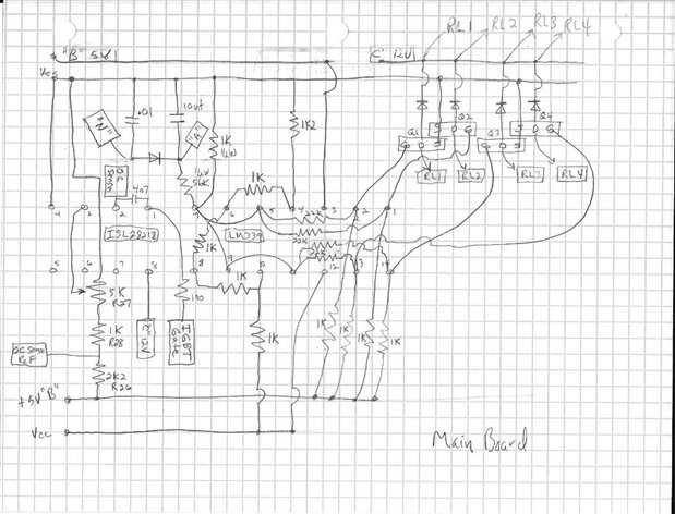
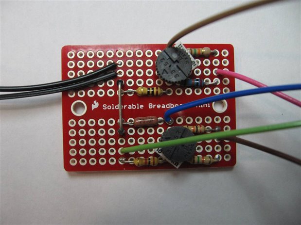
The first schematic is what I am calling the main board. Some of this schematic will actually be on a circuit board and the rest will be components mounted on the chassis of the unit or on the control panel. The boards I am using are solderable breadboards that will work adequately for the level of complexity and precision needed for this project. I am also going to publish my hand drawings of component layout on the boards. While these will be somewhat difficult to read and interpret I want to emphasize the importance of planning before actual construction.  These are my attempt at planning. As much as possible these schematics have been prototyped on regular bread board and tested for proof of concept.


Main Board


image


Clicking on the Schematic Should enlarge it.


The design has (4) series 0.5 ohm resistors that are each normally shorted out by relays. Also in series with the 4 resistors is a MOSFET and a 0.5 ohm current sense resistor. As the input voltage is applied and increased to the unit relays will open one after another adding 0.5 ohms of series resistance to the circuit. An LM339 comparator is being used  to drive gate level MOSFETs which in turn drive the relays. The reference inputs of the LM339 are set by a resistive divider so that relay 4 opens at 6 volts, relay 3 opens at 12 volts, relay 2 opens at 18 volts, and relay 1 opens at 24 volts. While it has been pointed out to me that properly heat sunk MOSFETs will eliminate the need for these resistors I wanted the exercise of seeing if I could design this type of approach.


U1 is a ISL28218 Rail to Rail OpAmp that controls the main Power MOSFET using the voltage level across the sense resistor and a reference voltage adjusted by 10 turn 5K R27. I am using the 5 volt supply for my reference voltage even though Peter has taught me better (should be an REF02). The precision of a unit is however only as good as the weakest link and the last time that I checked the "operator" of this unit has a tolerance of 10%.


The relays RL5 and RL6 are mounted to the chassis of the unit. RL5 ensures that there is support power to the circuitry of the unit before "Test Voltage" is connected. RL6 is tied back to the Limits Board which checks for Polarity of input "Test Voltage" as well as monitoring over voltage and over current faults. RL6 is a latching relay and when triggered disengages "Test Voltage" from all of the circuitry except the Volt Meter. SW1 is a manual reset of the latch.


Here are the hand drawn circuit board layouts for this schematic:


image


image


The next Schematic that will be covered is the Power Supply board for the unit. The schematic was drawn with the anticipation of finding a multiple secondary transformer which never materialized so the unit will be constructed with two transformers.


image


One of the things that I wanted to explore with the power supply board was the use of Recom's R78 series DC/DC switching convertors. These are great substitutes for the traditional linear 78XX series of voltage regulators. You will see when I cover actual board construction that while a tad bigger than the 78XX linear series the fact that no heat sink is needed more than makes up for the slightly larger size. I encourage you to check out these components on the Newark sales site. The 9 volt supply on the board is for the power to the meters. The meters that I chose to use require 9 volt isolated supplies. Since each meter only draws 0.5 mA I used a conventional linear regulator in a TO92 case for this application.


Here is the board layout for the Power Supply:


image


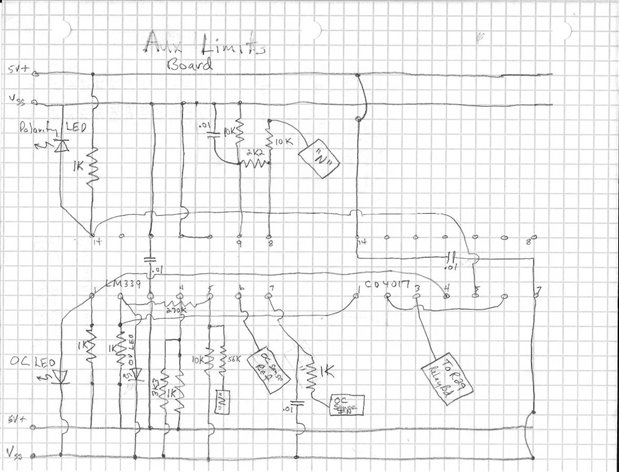
The next schematic that will be covered is for the Limits Board. This is where such fault conditions as Over Voltage, Over Current, and Polarity Reversal are detected and acted upon.


image


In this circuit we are using an LM339 comparator to measure the Fault Limit condition and feeding the gate outputs to a couple of OR gates which in turn will trigger RL6. The status of the failure is communicated to the front panel where LEDs indicate whether it is Polarity, OV, or OC that is causing the fault.


Here is the board parts layout for the Limits Board:


image


The last board in the unit is the meters interface and calibration board.


image


The purpose of this circuit is to take the 0V to 35V input of the unit and the voltage across the sense resistor and convert it to the proper voltage to be displayed by the 200mV full scale meters. The voltmeter will display 0.0 to 199.9 volts and the ammeter will display 0.00 amps to 19.99 amps though the upper range of this capability will hopefully never be displayed. The calibration is accomplished with a resistive divider that allows an adjustment of + or - a little over 10% of calculated top dead center.


Here is the parts layout for the board:


image


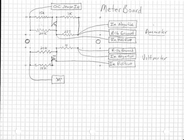
I will be covering construction of the boards in future Episodes but since the Meter Board has already been produced here is a preview.:


image


Sorry this got a little long but thanks for looking.


John

  • Sign in to reply

Top Comments

  • DAB
    DAB over 10 years ago +1
    Nice Blog John I look forward to seeing you test out the circuit. DAB
  • Robert Peter Oakes
    Robert Peter Oakes over 10 years ago +1
    Hi John, this is an excelent post, I like it and have taken a copy of the schematic for future reference, a few good ideas in there I can adapt to my project so stay tuned The thing about those power resistors…
  • Robert Peter Oakes
    Robert Peter Oakes over 10 years ago in reply to mcb1 +1
    Now that you mention that, Mikes electricstuff showed a video with almost that and a bucket of water rather than a fan Dummy load in a bucket Enjoy
  • Robert Peter Oakes
    Robert Peter Oakes over 10 years ago in reply to mcb1

    Now that you mention that, Mikes electricstuff showed a video with almost that and a bucket of water rather than a fan


    Dummy load in a bucket

    Enjoy image

    • Cancel
    • Vote Up +1 Vote Down
    • Sign in to reply
    • More
    • Cancel
  • jw0752
    jw0752 over 10 years ago in reply to Robert Peter Oakes

    Thanks Peter

    • Cancel
    • Vote Up 0 Vote Down
    • Sign in to reply
    • More
    • Cancel
  • mcb1
    mcb1 over 10 years ago in reply to Robert Peter Oakes

    as power resistors are or can be expensive

    Nothing like Nichrome wire and a fan ....

    • Cancel
    • Vote Up 0 Vote Down
    • Sign in to reply
    • More
    • Cancel
  • Robert Peter Oakes
    Robert Peter Oakes over 10 years ago

    Hi John, this is an excelent post, I like it and have taken a copy of the schematic for future reference, a few good ideas in there I can adapt to my project so stay tuned image


    The thing about those power resistors is that it off loads the required heat dissipation from the FET so you could use a lower powered one (Not less volts or current handling but less heat dissipation) as some of the heat will be going out through those resistors.

    At the end of the day though, you still have to get rid of the heat somehow and 30V at 5Amps nomatter how your distribute it is still 150Watts of heat going into the air, either the resistors can take more of it or the FETs will have to, the alternate is to parallel up the FETs to share the load and this nowadays may even be cheaper as power resistors are or can be expensive, Also there would be less mechanical switching in the form of the relays or complexity of the additional comparators

    As an educational / learning effort is is an excelent project and if you have all the parts then great, you will have a very usable tool at the end of it.


    One of the things I am looking to integrate into my next version is the ability to switch in different sense resistors to select different ranges without sacrifcing precision or dynamic range... something you could do easily with your version too if you want.


    Anyway, great post and I look forward to progress

    • Cancel
    • Vote Up +1 Vote Down
    • Sign in to reply
    • More
    • Cancel
  • jw0752
    jw0752 over 10 years ago in reply to michaelkellett

    Hi Michael,

    Thanks again for pointing out a weak spot in my design. After looking things over carefully I moved the Vdd of the LM 339 to the 12 volt supply. I changed R1 back to 1K and set up a bread board of the circuit. My switch points were at 6.8 Volts, 12.6 volts, 18.4 volts, and 24.2 volts with about  one volt lower for each point to switch off due to planned hysteresis. I left the open collector at 5 volts so as not to stress the gates of the NTD4906. I will also be moving the Vdd of the LM339 on the Limit board to the 12 volt supply. This is a much more robust design now. Here is a picture of the revised circuit on a bread board.


    image


    John

    • Cancel
    • Vote Up 0 Vote Down
    • Sign in to reply
    • More
    • Cancel
>
element14 Community

element14 is the first online community specifically for engineers. Connect with your peers and get expert answers to your questions.

  • Members
  • Learn
  • Technologies
  • Challenges & Projects
  • Products
  • Store
  • About Us
  • Feedback & Support
  • FAQs
  • Terms of Use
  • Privacy Policy
  • Legal and Copyright Notices
  • Sitemap
  • Cookies

An Avnet Company © 2026 Premier Farnell Limited. All Rights Reserved.

Premier Farnell Ltd, registered in England and Wales (no 00876412), registered office: Farnell House, Forge Lane, Leeds LS12 2NE.

ICP 备案号 10220084.

Follow element14

  • X
  • Facebook
  • linkedin
  • YouTube