


It isn't uncommon for me to find myself in need of a Pulse Width Modulation (PWM) signal in some of my bench experiments. Up until now I have put together a breadboarded PWM generator and modified it to suit my needs. The results always looked like this:

This project will be to design and build a board with the flexibility to cover the majority of my needs with respect to PWM under experimental conditions. Here are my list of requirements:
PWM Duty Cycle near 0% to near 100%
Adjustable frequency of operation
Integrated FET outputs. Gate Level Vth and up to 60 Vds
Adjustable PWM output
Sufficient Test Points to allow easy monitoring of circuit.
I begin the process with a test schematic that eventually evolves into a finished rendition of the circuitry of the project.

From the schematic I choose an appropriate sized board and create a parts layout with associated wiring. I have found that graph paper works well for this as the holes in the board correspond to the cross points on the graph paper. I put coordinates on the grid so that I have a reference to the board. For this project I am using an AdaFruit prototyping board. You can see this layout plan in the first picture above. Once I have a plan for component layout I begin to put the components onto the actual board. At first I will not solder as I have learned that real world problems and conflicts will show themselves that I didn't anticipate on the paper plan. Here is the board as the parts are beginning to be laid out.

Most of the components were individual but for the two FETs that I had determined would be necessary to meet my specifications I would have to make an assembly. The IRF 511 would mount to a heat sink with compound and a screw but the NTD 4906 would have to be soldered to the sink. I began by soldering the NTD 4906 to the small copper sink and then using the holes of the board for alignment I marked and drilled the mounting hole for the IFR 511. You can see this assembly in this picture.
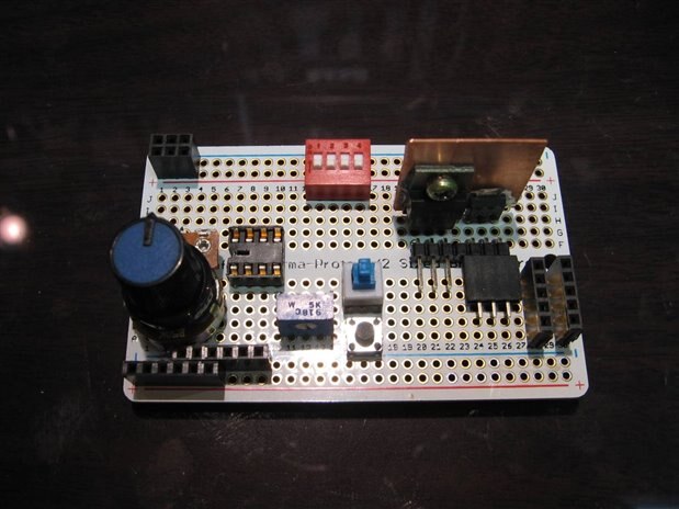
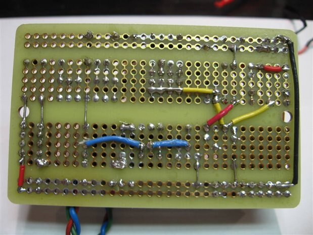
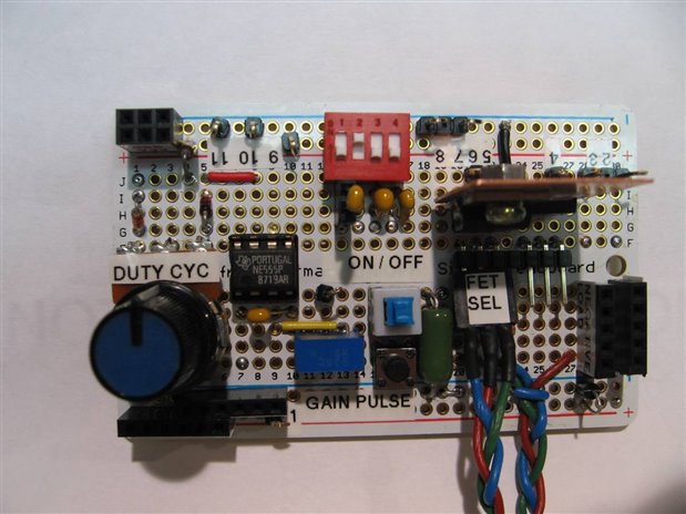
Since I had two possible FETs I decided that the easiest way to select between them would be a wire harness with a plug on the end to attach to one FET or the other. The header and plug in the above picture show the beginning of this concept. Once I have all the components positioned so that there are no serious conflicts I solder them to the board. Next, using the schematic for a guide, I work my way pin to pin around each of the components and make sure the proper circuit connections are made. It is important to check these and related connections several times. Even under the best conditions I seldom get it right the first time. Under worst case situations I may get some magic smoke when I run my first power up and have to go back and repair my mistakes. This time I was lucky. My preliminary powered tests showed the need for a resistor R-3 to pull the charge off the FET's gates when the gate coupling switch is turned off but no smoke. Here are pictures, front and back, of the finished circuit board without labels.

In my goals I mentioned the need for sufficient TEST POINTS to enable easy testing and monitoring of the circuit. When I finished there were 12 test points. I made the actual connections using header pins that I bent over so the test clips would not slide off. These TEST POINTS will also possibly serve as outputs to other circuits.
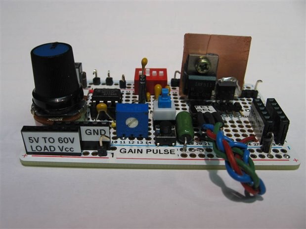
Pin 1 - + Voltage being supplied to the FET output circuit. 0 to 60 VDC for the IRF511 or 0 to 30 Volts for the NTD4906.
Pin 2 - This is the positive terminal output to the load.
Pin 3 - Negative Load connection
Pin 4 - Source connection on the NTD4906
Pin 5 - Source connection on the IRF511
Pin 6 - Drain connection on the FETs and the common connection to the heat sink
Pins 7, 8, 10, & 11 - Common Ground connection points for the circuit.
Pin 9 - + Voltage being supplied to the NE555 need from 5 volts to 15 volts
Pin 12 - PWM Output of the NE555 as controlled by VR-2. This is Isolated from the FETs if SW-2 and SW-3 are open.
Note: While the IRF511 will actually handle over 200 volts I did not feel that this board had the necessary safety protocols for this high a voltage therefore the recommended 60 volt input cap.
The frequency of the NE555 is to be controlled with a choice of capacitor. For this design I used a 4 gang DIP to select the required capacitor. In the first position I put a 2 pin header jack so that I could choose my own value for C-1. The position C-2, C-3, and C-4 have capacitors that correspond to 2 kHz, 20 kHZ, and 150 kHz respectively. The red DIP switch in the picture above provides this control.
The Duty Cycle of the PWM circuit is controlled by VR-1 which is the potentiometer in the lower left of the above picture. The small blue trimmer to the right is VR-2 and controls the amplitude of the output of the 555. This output can either be extracted through Test Pin 12 or it can be switched using the momentary push button SW-2 or SW-3 to drive the gates of the integral FETs.
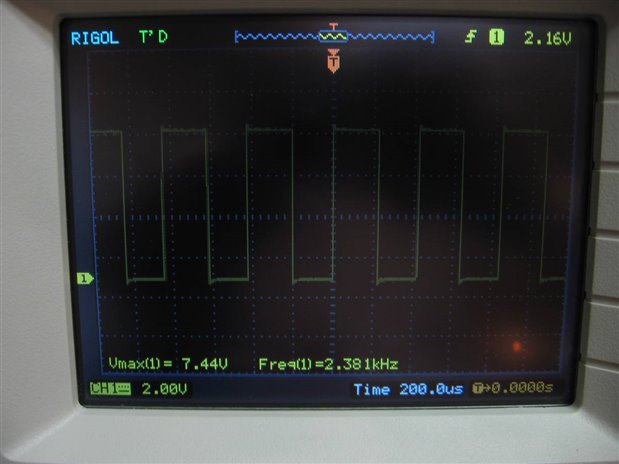
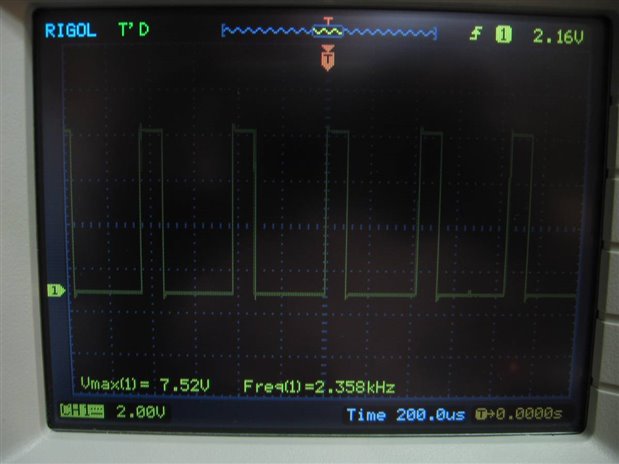
Here is a picture of the circuit under test. Please note the small Bread Board voltmeters Shop Tips - Bread Board Voltmeter are in use in this project. The light bulb is an automotive tail/brake light that I have wired with bread board leads so that I can use it as a simple resistive load. Unlike a regular resistor there is some insulation from the heat and I have a visual indicator of the approximate current.

In this case we have the NE555 running on 9.48 Volts and the voltage to the load is from an unregulated power supply that has settled at 12.7 volts under load. During this test I used VR-1 to change the Duty Cycle of the PWM . Here are the scope traces for three different duty cycles. I apologize for the quality of the screen shots as I just took pictures and did not bother with actually making captures.

I continued testing the unit until I was satisfied that it was working within expected parameters. My final step in each of these projects is to print my schematics and notes. I also usually write a detailed description of the circuit, how it works, what its intended purpose was, and as much other detail as possible. Experience has taught me that what is perfectly obvious to me today is often a difficult puzzle 6 months later. The notes, schematic, instructions and pictures are then made up into a booklet similar to an owners manual. Here are a couple pictures of the final LABELED board. Remember I label everything.
John.
Top Comments