

In the last blog about this board, I talked a little about the PSRAM chips. This blog is about getting them working and some digression into memory controllers in general.
I have two AP Memory APS6404 chips on the board and directly attached to the FPGA. The 4 data IO pins one each memory chip have their own FPGA pins but the chips elect and clock for each PSRAM share FPGA pins. The idea is to read and write data in 16-bit words to get a faster throughput.
If you want to really get into the detail of these chips then you will need to read the data sheet – which is readily obtainable, just search the part number.
In common with many similar chips the 6404 has a significant overhead each time a random memory address is selected. It can transfer one nibble of data per clock cycle once it gets going, so at first glance you might expect to achieve read and write speeds of up to 133/2 Mbyte/s (the headline max clock is 133MHz).
For speed the chip will always be operated in quad mode so for the following discussion it is assumed that this is the case.
To write to n bytes memory you must send two nibbles of write command, 6 nibbles of address and 2n nibbles of data. (2 nibbles = 1 byte). Any real controller will have a little overhead of its own, my controller and test core require 6 clock cycles per write operation.
Read operation are worse in that they need send two nibbles of read command, 6 nibbles of address and 6 clock cycles of wait time before any read data can be clocked out.
The effect of the overhead can be reduced by reading or writing bursts of many bytes but there are some issues that need to be considered.
The first is that the 6404 only allows a maximum length of data burst of 32 bytes at clock rates above 84MHz.
The maximum permitted chip enable time is 4us for extended temperature range parts and 8us for normal range parts. This sets the maximum burst length for any clock rate to just over 300 bytes.
When you take all these things into account you can work out how fast data can be transferred.

Operating the chip at 133MHz is not straightforward. The clock cycle time is 7.5ns and the chip needs data setup and hold times of 4ns total. This does not leave much margin for skew and delay in the driving circuits. AP Memory recommend active tuning to get it right.
On this board, which uses unmatched length tracks and low cost board I sidestep the issue by clocking at 75MHz.
This should allow a maximum read rate of 36.09Mbyte/s, doubled because I have two chips effectively in parallel.
Test Controller Architecture
At the very lowest level the controller architecture is quite simple.
The internal interface has inputs for address, burst length, write data and start, and outputs for read data and busy.
All my internal VHDL logic operates on the rising clock edge. The simplest way of clocking the memory chips is to use the inverse of the main clock, gated as required, to meet the timing requirements of the 6404 for control and data edges relative to clock edges.
The low-level interface is called psram_access because it isn’t really a controller. For testing purposes its driven by a test block which writes 16 bursts of 32 16-bit words to memory. The data is the inverse of the low order 16 bits of the address. The test block then reads the data back and checks it, finally setting the good or bad signals as appropriate.
Top level of design used for simulation and testing

PSRAM Control Block

VHDL Code for psram_access module
-------------------------------------------------------------------------------
--
-- Title       : psram_access
-- Design      : EFTB
-- Author      : Michael Kellett
-- Company     : MK Electronics Ltd
--
-------------------------------------------------------------------------------
--
-- File        : C:\Docs\Rabbits\Efinix_EFTB_rtl\Aldec\src\psram_access.vhd
-- Generated   : Sun Jan  1 14:15:49 2023
-- From        : interface description file
-- By          : Itf2Vhdl ver. 1.22
--
-------------------------------------------------------------------------------
--
-- Description :
--
-------------------------------------------------------------------------------

--{{ Section below this comment is automatically maintained
--   and may be overwritten
--{entity {psram_access} architecture {psram_access}}

library IEEE;
use IEEE.std_logic_1164.all;
use IEEE.NUMERIC_STD.all;

entity psram_access is
	 port(
		 clk75 : in STD_LOGIC;
		 res_hi : in STD_LOGIC;
		 r_nwr : in STD_LOGIC;
		 transfer : out STD_LOGIC;
		 start : in std_logic;
		 psr_dat_i : in std_logic_vector(7 downto 0);
		 psr_nce : out std_logic;
		 psr_clk : out std_logic;
		 busy : out std_logic;
		 length : in STD_LOGIC_VECTOR(10 downto 0);
		 read_data : out STD_LOGIC_VECTOR(15 downto 0);
		 write_data : in STD_LOGIC_VECTOR(15 downto 0);
		 address : in STD_LOGIC_VECTOR(23 downto 0);
		 psr_dat_o : out STD_LOGIC_VECTOR(7 downto 0);
		 psr_out_en : out STD_LOGIC_VECTOR(7 downto 0);
		 psr_debug : out STD_LOGIC_VECTOR(7 downto 0)
	     );
end psram_access;

--}} End of automatically maintained section

architecture psram_access of psram_access is

	signal command : std_logic_vector(7 downto 0);
	signal bit_count : unsigned(4 downto 0);
	signal address_sr : std_logic_vector(23 downto 0);
	signal n_words : unsigned(10 downto 0);
	signal read_reg : std_logic_vector(15 downto 0);
	signal write_reg : std_logic_vector(15 downto 0);
	signal quad : std_logic;
	signal psr_clk_en : std_logic;

 	TYPE t_psa_state is (PSA_IDLE, PSA_CMND_1, PSA_CMND_2, PSA_CMND_3, PSA_WRITE_1, PSA_WRITE_2, PSA_WRITE_3, PSA_READ_1, PSA_READ_2, PSA_READ_3, PSA_READ_4,
	PSA_QUAD_1);
	signal psa_state : t_psa_state;


begin

	 -- enter your statements here --

	psram : process(clk75)
	begin
		if rising_edge(clk75) then
			if res_hi = '1' then
				psr_nce <= '1';
				psr_out_en <= (others => '0');
				busy <= '0';
				quad <= '1';
				transfer <= '0';
				psa_state <= PSA_IDLE;
			else
				if psa_state /= PSA_IDLE then
					psr_clk_en <= '1';
				else
					psr_clk_en <= '0';
				end if;
				case psa_state is
					when PSA_IDLE =>
					if start = '1' or quad = '1' then
						busy <= '1';
						if quad = '1' then
							command <= "00110101";		-- quad mode command
						elsif r_nwr = '1' then
							command <= "11101011";		-- read command
						else
							command <= "00111000";		-- write command
						end if;
						if quad = '1' then
							psr_out_en <= "00010001";		-- enable drive on SI pins on both PSRAMS
						else
							psr_out_en <= "11111111";
						end if;
						bit_count <= "00000";			-- will count serial bits sent
						address_sr <= address;
						n_words <= (others => '0');
						psa_state <= PSA_CMND_1; 		-- will start clock
					end if;
				when PSA_CMND_1	=>
--					psr_nce <= '0';						-- chip select asserted
					psa_state <= PSA_CMND_2;
				when PSA_CMND_2 =>
					psr_nce <= '0';						-- chip select asserted
				    if quad = '0' then
						psr_dat_o(3 downto 0) <= command(7 downto 4);			-- already in quad mode
						psr_dat_o(7 downto 4) <= command(7 downto 4);	  		-- send ms nibble out on SPI to PSRAMS
						command(7 downto 4) <= command(3 downto 0);	 			-- prepare next nibble to send
						if bit_count = 1 then
							bit_count <= "01000"; 								-- correct bit count (to 8) in case of using spi mode (currently not coded)
							psa_state <= PSA_CMND_3;							-- move on to address sending in 4 bit nibbles
						else
							bit_count <= bit_count + 1;							-- NB - won't change bit_count before it gets checked in next line
						end if;
					else
						psr_dat_o(0) <= command(7);								-- in spi_mode
						psr_dat_o(4) <= command(7);
						command(7 downto 1) <= command(6 downto 0);	 			-- prepare next bit to send
						bit_count <= bit_count + 1;			-- NB - won't change bit_count before it gets checked in next line
						if bit_count = 7 then				-- will send 8 bits in spi mode
							psa_state <= PSA_QUAD_1;		-- if was only getting into quad mode using spi then it's done
						end if;
					end if;
				when PSA_CMND_3 =>
					psr_dat_o(3 downto 0) <= address_sr(23 downto 20);
					psr_dat_o(7 downto 4) <= address_sr(23 downto 20);
					address_sr(23 downto 4) <= 	address_sr(19 downto 0);
					bit_count <= bit_count + 1;			-- NB - won't change bit_count before it gets checked in next line
					if bit_count = 13 then
						if r_nwr = '1' then
							psa_state <= PSA_READ_1;
						else
							psa_state <= PSA_WRITE_1;
						end if;
					end if;
				when PSA_READ_1 =>
					bit_count <= bit_count + 1;			-- NB - won't change bit_count before it gets checked in next line
					if bit_count = 20 then	 			-- 6 wait states for read tweaked from +6 to + 7
						psa_state <= PSA_READ_2;
					end if;
					if bit_count = 14 then 				-- going to read so disable drivers
						psr_out_en <= "00000000";
					end if;
				when PSA_READ_2 =>
					transfer <= '0';									-- clear FIFO write if reading subsequent word
					read_reg(15 downto 12) <= psr_dat_i(7 downto 4);
					read_reg(7 downto 4) <= psr_dat_i(3 downto 0);	-- buffer the ms nibbles
					n_words <= n_words + 1;
					psa_state <= PSA_READ_3;
				when PSA_READ_3 =>
					read_data(11 downto 8) <= psr_dat_i(7 downto 4);
					read_data(3 downto 0) <= psr_dat_i(3 downto 0);
					read_data(7 downto 4) <= read_reg(7 downto 4);
					read_data(15 downto 12) <= read_reg(15 downto 12);
					transfer <= '1';  									-- write data to FIFO
					if n_words = unsigned(length) then
						psr_nce <= '1';
						psa_state <= PSA_READ_4;
					else
						psa_state <= PSA_READ_2;
					end if;
				when PSA_READ_4 =>
					transfer <= '0';
					busy <= '0';
					psa_state <= PSA_IDLE;


				when PSA_WRITE_1 =>						-- no wait states needed
					write_reg <= write_data;
					psr_dat_o(7 downto 4) <= write_data(15 downto 12);
					psr_dat_o(3 downto 0) <= write_data(7 downto 4);
					transfer <= '1';
					n_words <= n_words + 1;
					psa_state <= PSA_WRITE_2;
				when PSA_WRITE_2 =>
					transfer <= '0';
					psr_dat_o(7 downto 4) <= write_reg(11 downto 8);
					psr_dat_o(3 downto 0) <= write_reg(3 downto 0);
				    if n_words = unsigned(length) then
						psa_state <= PSA_WRITE_3;
					else
						psa_state <= PSA_WRITE_1;
					end if;
				when PSA_WRITE_3 =>
					psr_nce <= '1';
					busy <= '0';
				    psa_state <= PSA_IDLE;


				when PSA_QUAD_1 =>
					psr_nce <= '1';
					busy <= '0';
					quad <= '0';
					psr_out_en <= (others => '0');
				    psa_state <= PSA_IDLE;

				when others =>
					psr_nce <= '1';
					busy <= '0';
				    psa_state <= PSA_IDLE;
				end case;
			end if;
	   end if;
	end process;

	psr_debug <= psr_dat_i;
	psr_clk <= '0' when psa_state = PSA_IDLE else (not clk75);

end psram_access;
VHDL Code for psram_test module
-------------------------------------------------------------------------------
--
-- Title       : psram_test
-- Design      : EFTB
-- Author      : Michael Kellett
-- Company     : MK Electronics Ltd
--
-------------------------------------------------------------------------------
--
-- File        : C:\Docs\Rabbits\Efinix_EFTB_rtl\Aldec\src\psram_test.vhd
-- Generated   : Tue Jan  3 09:25:57 2023
-- From        : interface description file
-- By          : Itf2Vhdl ver. 1.22
--
-------------------------------------------------------------------------------
--
-- Description :
--
-------------------------------------------------------------------------------

--{{ Section below this comment is automatically maintained
--   and may be overwritten
--{entity {psram_test} architecture {psram_test}}

library IEEE;
use IEEE.std_logic_1164.all;
use IEEE.NUMERIC_STD.all;

entity psram_test is
	 port(
		 clk75 : in STD_LOGIC;
		 res_hi : in STD_LOGIC;
		 start_test : in STD_LOGIC;
		 ps_busy : in std_logic;
		 good : out STD_LOGIC;
		 bad : out STD_LOGIC;
		 ps_start : out STD_LOGIC;
		 r_nwr : out STD_LOGIC;
		 transfer : in STD_LOGIC;
		 length : out STD_LOGIC_VECTOR(10 downto 0);
		 write_data : out STD_LOGIC_VECTOR(15 downto 0);
		 read_data : in STD_LOGIC_VECTOR(15 downto 0);
		 address : out STD_LOGIC_VECTOR(23 downto 0)
	     );
end psram_test;

--}} End of automatically maintained section

architecture psram_test of psram_test is

	signal length_reg : unsigned(10 downto 0);
    signal address_reg : unsigned(23 downto 0);
	signal wr_val : unsigned(15 downto 0);
	signal n_blocks : unsigned(7 downto 0);
	signal timer : unsigned(15 downto 0);
	signal read_errs : unsigned(23 downto 0);


	constant K_LENGTH : unsigned(10 downto 0) := "00000100000";			-- will use 32 word bursts to write

 	TYPE t_test_state is (PS_TST_IDLE, PS_TST_WRITE_0, PS_TST_WRITE_1, PS_TST_WRITE_2, PS_TST_WRITE_3, PS_TST_WRITE_4, PS_TST_READ_1, PS_TST_READ_2, PS_TST_READ_3, PS_TST_READ_4, PS_TST_READ_5);
	signal test_state : t_test_state;

begin

	-- enter your statements here --
	psram_test : process(clk75)

	variable new_wr_val : unsigned(15 downto 0);
	begin
		if rising_edge(clk75) then
			if res_hi = '1' then
				good <= '0';
				bad <= '0';
				ps_start <= '0';
				length <= std_logic_vector(K_LENGTH);
				test_state <= PS_TST_IDLE;
			else
				case test_state is
					when PS_TST_IDLE =>
					if start_test = '1' then
						good <= '0';
						bad <= '0';
						wr_val <= (others => '0');
						r_nwr <= '0';						-- write mode
						n_blocks <= (others => '0');
						address_reg <= (others => '0');
						test_state <= PS_TST_WRITE_0;
					end if;

					when PS_TST_WRITE_0 =>
						address <= std_logic_vector(address_reg);
						write_data <= not std_logic_vector(wr_val);		   	-- write data = (not address(15 downto 0) )
						test_state <= PS_TST_WRITE_1;

					when PS_TST_WRITE_1 =>
					if ps_busy = '0' then  					-- wait until access block is not busy
						ps_start <= '1';	 				-- start the write
						n_blocks <= n_blocks + 1;			-- count of blocks of length words written
						test_state <= PS_TST_WRITE_2;
					end if;

					when PS_TST_WRITE_2 =>
					if ps_busy = '1' then  					-- wait until access block is busy (ie has responded to start signal)
						ps_start <= '0';
						test_state <= PS_TST_WRITE_3;
					end if;


					when PS_TST_WRITE_3 =>
					if transfer  = '1' then					-- if the access block has read the data word
						new_wr_val := wr_val + 1;			-- calc new one
						write_data <= not std_logic_vector(new_wr_val);	 -- and output it
						wr_val <= new_wr_val;
					elsif ps_busy = '0' then 					-- the data block has been written
						if n_blocks = 16 then
							test_state <= PS_TST_WRITE_4;
						else
							address_reg <= address_reg + ("000000000000" & K_LENGTH); 		-- add block length to address
							test_state <= PS_TST_WRITE_0;
						end if;
					end if;

					when PS_TST_WRITE_4 =>
						timer <= "0000010111011100";  	--1500;
						test_state <= PS_TST_READ_1;

					when PS_TST_READ_1 =>
					if timer = 0 then
						wr_val <= (others => '0');
						r_nwr <= '1';						-- read mode
						n_blocks <= (others => '0');
						address_reg <= (others => '0');
						test_state <= PS_TST_READ_2;
						read_errs <= (others => '0');
					else
						timer <= timer - 1;
					end if;

					when PS_TST_READ_2 =>
					if ps_busy = '0' then
						address <= std_logic_vector(address_reg);
						n_blocks <= n_blocks + 1;			-- count of blocks of length words written
						ps_start <= '1';	 				-- start the write
						test_state <= PS_TST_READ_3;
					end if;

					when PS_TST_READ_3 =>
					if ps_busy = '1' then  					-- wait until access block accepts start
						ps_start <= '0';
						test_state <= PS_TST_READ_4;
					end if;

					when PS_TST_READ_4 =>
					if transfer = '1' then
						if std_logic_vector(wr_val) /= not read_data then
							read_errs <= read_errs + 1;
						end if;
						wr_val <= wr_val + 1;
					elsif ps_busy = '0' then
						if n_blocks = 16 then
							test_state <= PS_TST_READ_5;
					    else
							address_reg <= address_reg + ("000000000000" & K_LENGTH); 		-- add block length to address
							test_state <= PS_TST_READ_2;
						end if;
					end if;

					when PS_TST_READ_5 =>
					if read_errs = 0 then
						good <= '1';
					else
						bad <= '1';
					end if;
					test_state <= PS_TST_IDLE;


					when others =>
						good <= '1';
						bad <= '1';
					    test_state <= PS_TST_IDLE;
				end case;
			end if;
	   end if;
	end process;


end psram_test;
Extract from Simulation

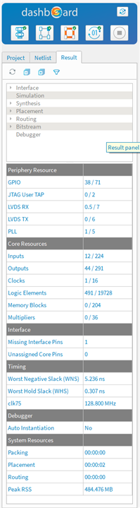
Efinix Dashboard
Test Results Using Logic Analayser
Write burst

Final read burst - sets 'good' signal

Start of final read burst - can be compared with simulation results

Architecture of more useful controllers
The very simple setup described so far is fine to test that the ram chips are correctly connected, and that the FPGA can drive them at a useful speed.
A much more complex controller is required to do anything useful.
This is because the memory must be read or written in bursts to get any thing loke its best performance.
Suppose we want to use the memory as a buffer for a data acquisition system that will gather data from, for example, a multichannel ADC and send it on via a Gbit Ethernet interface.
We will need a write port and a read port which must operate simultaneously as far as the world outside the controller is concerned.
This can be done by buffering the write data in a FIFO using on FPGA memory and writing bursts of data to the memory. Data can be read from the memory into a second FIFO which may be read by the Ethernet controller. The memory controller must share the memory bandwidth between the two ports. This is a simple situation because both read and write are to/from sequential addresses. In a real application there may be requests from the Ethernet controller for out of sequence blocks of data if packets should be lost.
A huge jump in complexity occurs if non-sequential blocks of data must be written or read because the memory controller FIFO s must now store block lengths and addresses along with the data.
MK
Top Comments
-

shabaz
-
Cancel
-
Vote Up
0
Vote Down
-
-
Sign in to reply
-
More
-
Cancel
-

michaelkellett
in reply to shabaz
-
Cancel
-
Vote Up
+1
Vote Down
-
-
Sign in to reply
-
More
-
Cancel
-

shabaz
in reply to michaelkellett
-
Cancel
-
Vote Up
0
Vote Down
-
-
Sign in to reply
-
More
-
Cancel
-

michaelkellett
in reply to shabaz
-
Cancel
-
Vote Up
0
Vote Down
-
-
Sign in to reply
-
More
-
Cancel
-

shabaz
in reply to michaelkellett
-
Cancel
-
Vote Up
0
Vote Down
-
-
Sign in to reply
-
More
-
Cancel
-

scottiebabe
in reply to shabaz
-
Cancel
-
Vote Up
0
Vote Down
-
-
Sign in to reply
-
More
-
Cancel
-

shabaz
in reply to scottiebabe
-
Cancel
-
Vote Up
0
Vote Down
-
-
Sign in to reply
-
More
-
Cancel
Comment-

shabaz
in reply to scottiebabe
-
Cancel
-
Vote Up
0
Vote Down
-
-
Sign in to reply
-
More
-
Cancel
Children