

I started this project a while ago (September 2024) but just picked it up again. To get the best out of this blog you will need to download the combined User and Service Manual for the HP59313A, which you can find at: https://www.keysight.com/us/en/assets/9018-02649/user-manuals/9018-02649.pdf
This manual is dated 1977 and you can still download it free from Keysight’s website. (HP spawned Agilent, which in turn spawned Keysight.) Kudos to them all !
If you stick with it, this blog will teach some interesting history, a bit about fault finding and open some doors to learning a lot about electronics.
What is an HP59313A
To understand it properly we need a little history.
In 1972 Hewlett Packard Inc (HP) announced the Hewlett Packard Interface Bus (HPIB) for interconnecting electronic instruments and computers (which HP still called calculators at that time) to enable the assembly of complex automatic test and measuring systems. This was two years before the first personal computer was announced (Altair 8800).
HP backed HPIB to the hilt and it became a feature of all their instruments. It was also adopted by other manufacturers and standardised as IEE-488 in 1975. HPIB became more widely known as GPIB.
There is a decent wiki article: https://en.wikipedia.org/wiki/GPIB
In the early years of GPIB many instruments were not compatible but there was still a demand to connect them, so HP made a set of interfaces of which the 59313A is one.
It’s a 4 input 200s/s ADC with 10 bit plus sign resolution.
There’s a great 1981 article showing how it was meant to be used: https://www.hpmemoryproject.org/an/pdf/an_155-3.pdf
The HP59313A was introduced in 1977 at $1500 and continued in production until the early 1990s.
It, and other members of the 59xxx series were interesting because they do not use micro- processors or controllers for digital functions but are implemented entirely with 74 series logic.
The HP59313A contains approximately 93 ICs, about 15 of them analogue.
Why bother fixing it ?
In its day a new HP59313A cost $1500 (approx. $8000 in today’s money) , for which you got a 4 input 11bit 200Hz ADC with a bus interface and some pretty limited signal conditioning.
But now you can buy a micro with a 12 bit 1MHz ADC for $1.
NI (not the cheapest guys on the block) will sell you a USB based rough equivalent (14 bit, 10kHz, 8 channel) for £247 (Farnell 3622270).
So you might feel that there was nothing to be learned from a 50 year old design – and if all you want to do is measure some signals as cheaply and simply as possible you might well be right.
But there is a huge amount to be learned from studying how electronic problems were solved when cheap embedded computing didn’t exist, and you couldn’t just buy an ADC chip. And that knowledge will help you understand the art of electronics do better work today.
I fixed mine, at least in part, because it’s an interesting puzzle. And also, because I didn’t want to feel I had wasted £40 ! But I have learned some interesting things along the way.
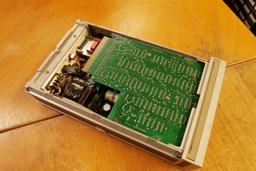
Taking the HP59313A apart.
There is a teardown on EEVblog
https://www.eevblog.com/forum/testgear/hp-59313a-half-teardown/
But that guy didn’t want to fix his so he misses the best bit.
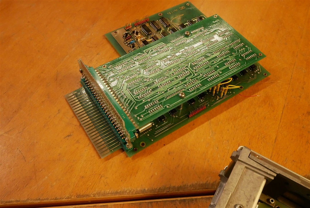
It uses the PCBs in 3 layer sandwich.
There’s a lot of logic on the middle board and all the components are on the “inside” faces of the sandwich so at first sight it looks like a bit of a monster to work on.
Pic of top/middle sandwich
Debug configuration
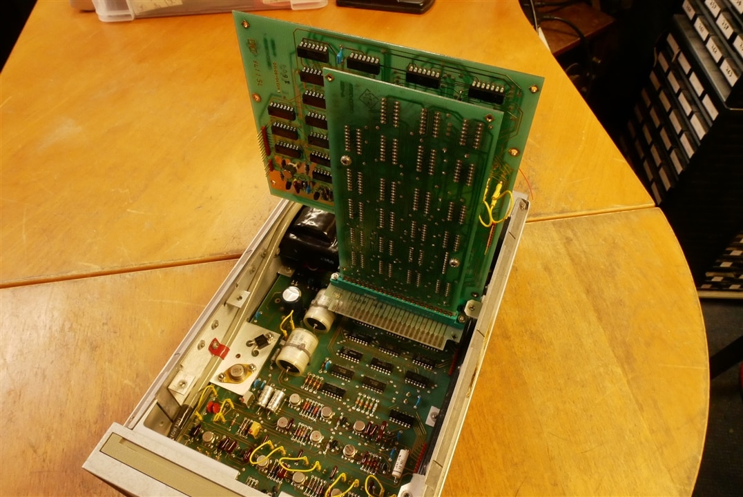
The HP guys thought about how you would fix it !
Debugging
I posted about this a long time ago in /members-area/personalblogs/b/michael-kellett-s-blog/posts/first-design-with-kicad-8-0
The first thing I did was take the covers off and look for smoked parts. There weren’t any so I powered it up and nothing happened (no lights, no smoke). Checking the power rails revealed no 5V DC supply but there was input to the regulator.
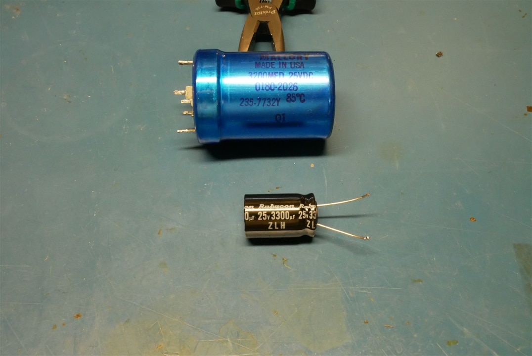
I replaced the LM309 linear voltage regulator with a 7805 and the 5V supply sort of worked. (5V with lots of 100Hz noise.) I had to replace the reservoir capacitor as well.
It’s quite amazing how much smaller the modern 3300uF 25V cap is compared with the original Mallory 3200uF part. (Not a typo – 3200uF). It isn’t just chips that have got smaller.
It still didn’t work even with good power supplies.
Debugging via GPIB
The HP59313A has no front panel controls – everything must be done via the bus. You can buy expensive adapters for PCs (made by Keysight, NI and others) which go from USB to GPIB.
A cheaper solution is the USB adapter from Prologix but its currently $300. Its an old design and contains about $20 worth of bits - I think they are resting on their laurels a bit.
It is popular and works quite well - I have one which I use for reference.
There are several designs on the web for DIY interfaces, but I hate taking the quick and simple route, so I designed my own !
It has features that the others don’t, mainly two connectors for a logic analyser (you’ll be seeing why soon).
But the main thing is that it’s my design and code so I can tweak it as I want – which leads us into another GPIB digression.
Old GPIB v modern GPIB
HP released HPIB as a hardware specification. Some protocol stuff is implied but its basically a way of transferring 8 bit bytes from one machine to another on a network of two or more. The very first instruments to use it (and the HP59313A is firmly in that category) had very limited processing power and used very simple protocols. After a few years (read the Wiki link) HP invented and adopted SCPI which is a big complex software protocol using the original HPIB as the physical layer.
A typical modern instrument would send back ADC data as text in floating point volts. The HP59313A sends it back like this:

The Prologix adapter rather expects a more modern instrument (it can just about cope with the HP59313A but it’s not ideal).
My interface now has an hp59313a mode of operation where it reads the data from the HP59313A and converts it to nice, signed decimal text strings.
GPIB is more than just the data bytes – timing and the 8 control lines matter too – which is why I have the logic analyser connections. It would be possible for the interface to double up as a bus analyser and I hear that the NI ones offer this - I can’t comment on it because I’ve never used one (and at £1741 a pop I’m not planning to !).
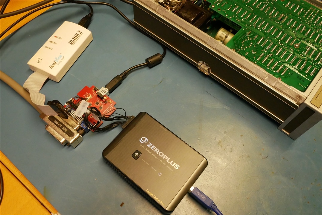
HPIB test rig, showing the approved way of using a home brew GPIB interface - connected to the processor debugger for on the fly improvements. The Zeroplus box is the logic analyser.
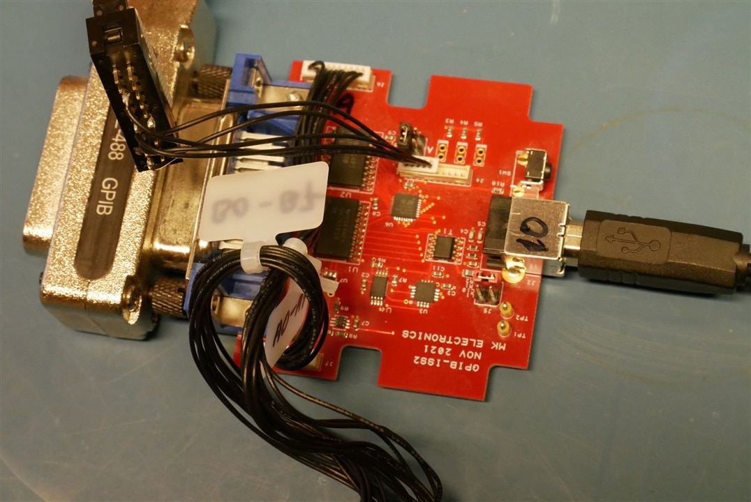
The GPIB interface. The two big chips are the bus interface buffers, the processor is the small QFN next to them.
Debugging the bus logic
The great thing about HP gear of this vintage is that you get the full parts list, schematics and a pretty good explanation of how the thing it supposed to work.
The way that they optimised the control codes to minimise the logic required is an object lesson in efficient design. No one would bother now – but an example won’t hurt !
The HP59313A uses single character control codes:
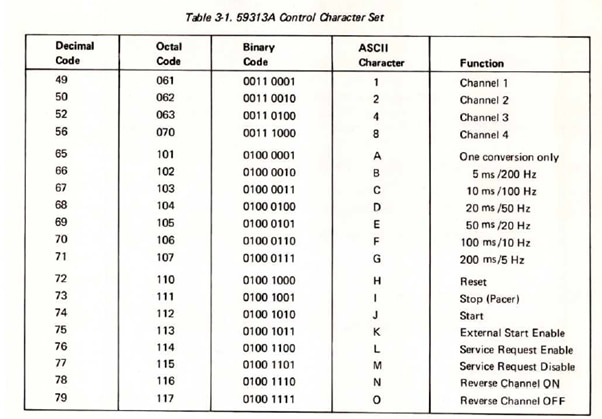
The table makes it clear how the decoding logic (and it is logic chips) will react to the binary encoding of the ascii command characters. So, by using 1,2,4,8 to select 1,2,3,4 they save a 4- way multiplexer .
There are several other examples in the guts of the logic where they slightly complicate one function to eliminate some logic elsewhere.
My HP59313A wouldn’t do any converting at all.
Looking at the bus when the controller sends the H (Reset) command the HP59313A doesn’t acknowledge it at all.
Pic of send H

Using the block diagrams and schematics gave me clues as to where to look and I found this on U26 on the top board:
Pic of U26 pins

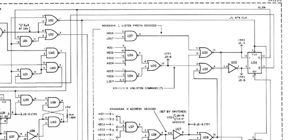
U31-9 = U26-13 which doesn’t toggle when it should.
I replaced U26 - it was as SN7473 but I replaced it with an LS part because n one seems to sell standard 74 series logic now.
Of course the HP59313A still didn’t work and I had to replace two more logic chips, another 7473 and a 7410. I found them using the same technique, but they were a bit easier.
This is the counter for the dual slope ADC trigger:
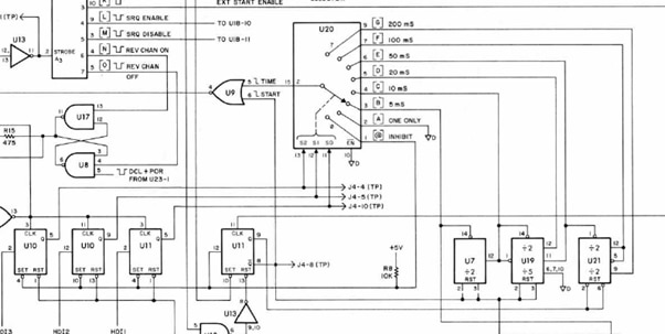
There was no clock on U20 pin 9 but 7, 6 etc were OK. A little scope probing showed U21 (7473) to have input but no output.
Once I replaced that chip it loked as if the HP59313A was working.
Testing the HP59313A
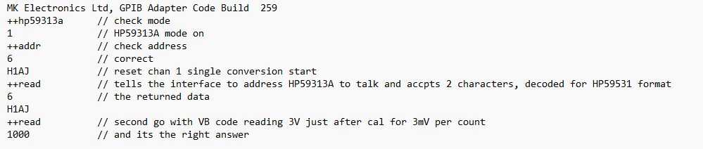
I wrote simple programme in VB6 (seems totally appropriate to use a language discontinued 25 years ago to test some hardware twice its age).
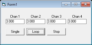
You can use any language you like, or even Hyperterminal.
Conclusions
Now that I've fixed it I'm not quite sure what to do with it next.
It was fun to do an interesting to get to understand it better. I've had to get little deeper into the GPIB and I think I may do a version 3 of my USB to GPIB adapter with a more powerful processor so it can support proper bus analysis.
Although slow it is quite a good 11 bit ADC with less than 1 lsb noise and it's in a nice box.
Like the guy on eevblog, I bought it for the box so I may end up binning the works !
It is a good way of learning electronics and while in theory you could just download lost of old service manuals and study them, I think you learn a lot more by actually getting stuck in and working on the hardware.
If you want to learn about electronic hardware buying and fixing old stuff is good way to do it.
Links
https://www.holzleitner.com/el/hp-59xxx/index-en.html
https://hparchive.com/Catalogs/HP-Catalog-1977.pdf

