



Introduction
I’m working on a wired remote-control system which must transfer a lot of data across a CAT6 cable with a very fast response .
We decided to use GB Ethernet which will allow us to pass power and data on the same reasonably priced cable .
The system is strictly point to point and no devices will be attached other than the Controller at one end and the Remote at the other. This means that we have no need to stick to conventional Ethernet formats and can avoid wasting bandwidth on transmitting MAC and IP addresses back and forth a million times per second.
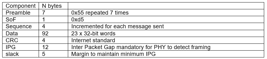
Basic Ethernet frames don’t include IP addresses but still use 14 bytes for MAC and frame type information.
For a frame to work at all it requires 7 bytes of pre-amble, 1 byte for the Start of Frame symbol and when it is done there must be an inter-packet gap of 12 bytes. Any sensible system will include a CRC (or similar) and some kind of message ID - we decided to stick with 4 bytes for both which results in an overhead of 28 bytes per frame. At 1GB/s we can send 125 bytes per us so 1 frame per us leaves 97 for data. (A 2 MHz frame rate may be possible but does lose 44% of the bandwidth to overhead.)
We decided to use a 1MHz frame rate which allows us 22 or 23 x 32-bit words of data (88 or 92 bytes), while still leaving a margin of 5 bytes per frame.
We didn’t want to design and build our own FPGA boards at this early stage in the project, so we chose the MicroPhase A7 Lite board which is fitted with an AMD Artix 7 FPGA and a Realtek 8211E GB Ethernet PHY.
The Realtek PHY would not normally have been our first choice because it is hard to get data directly, although a limited data sheet is quite widely available. This caused some problems later.
Initial Testing and a Big Problem
This is quite a big (by my standards) project, and it took a while to get all the code for the FPGA written to a level where any physical testing was possible. Then a whole load more code for the processor that tells the FPGA what to do.
So, it’s a big moment when finally, two boards are talking to each other, and transferring messages at the 1MHz rate.
One of the many functions of the system is that you can drive a pin at one end, and see the corresponding pin change at the other. And we very quickly noticed that, despite our 1MHz message rate and a lot of care in the FPGA design not to introduce lots of latency in buffers, the latency of the system was about 20us.
I added extensive monitoring to the FPGA design to try and pin down where the latency was being introduced. The simulation said that it was not coming from the FPGA. The only other place it could come from was the PHY, but that would mean that it had a buffer capable of storing more than 20,000 bits of data. The data sheet does not refer to such a buffer and the AIs I asked varied from “No it definitely can’t buffer that much data : Google AI mode” to “It almost certainly can’t but because of the secret data sheet thing we can’t be quite sure : Claude”. Both Google and Claude remarked on the interesting closeness of the observed latency to the recovery time from EEE Green Ethernet power saving mode. This can be switched off, but requires accessing the PHY control registers via MDIO interface – I had hoped not to need this so a but more FPGA work was required to add an MDIO interface controlled by the system processor via SPI.
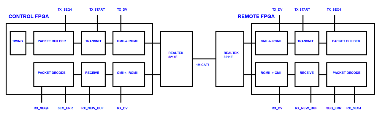
(above) A very much simplified block diagram showing the key FPGA subsystems and the sources of the debugging signals.
The two FPGA s and their boards are identical. A serial interface (not shown) allows a PC to set them up as Control or Remote.
The Control end enables the timing generator which will start a transmit packet every 1us in normal mode. It has test modes to allow the generation of short bursts of start pulses at varying rates. The remote end sends back a packet whenever it receives one, so the remote timing is synchronised with the Control end. This scheme only works if the PHY latency times are stable and short.
The packet builder builds up frames to transmit, which contain the useful system data and, important for error detection, the sequence word which increments for each frame. A debug pin is operated by bit 4 of the sequence word as it is transmitted and received – this provides a way of measuring the system latency.
The transmitter drives the ethernet frames out to the GMII to RGMII converter which in turn drives the PHY. The transmitter is clocked at the PHY data rate of 125MHz. RGMII is the interface standard used by the PHY and it transfers data on 4 pins on both rising and falling edges of the 125MHz clock. GMII is similar but transfers 8bits on the rising edge of the clock. Conversion from one to another of these standards requires some cunning hardware gymnastics performed by special IO features of the FPGA. (Most FPGAs have at least some output pins that can do double data rate IO.)
The TX_DV and RX_DV are the data valid signals for the GMII interface. They should be very close in timing to the corresponding signals on the RGMII.
(I didn’t attempt to connect directly to the PHY pins because of the physical difficulty of getting at them and I didn’t want to potentially mess up the DDR conversion by trying to access the pins from inside the FPGA – it turned out that the GMII signals were good enough.)
Bug Hunting Test set-up
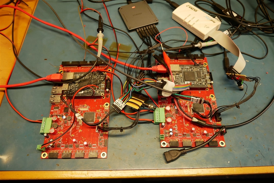
It needs two PCs, I had one running the Vivado FPGA design software, the Arm Keil MDK IDE for the on board processor, the Aldec simulator, the FRINSI logic analyser and a terminal emulator to talk to the Control end processor.
The other PC only has to talk to the remote end processor.
I used the recently acquired FNIRSI Logic Analyser to capture debug data from the FPGA.
Test Resuts
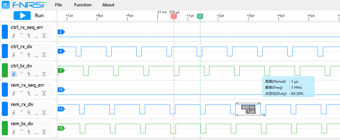
(above) Continuous 1MHz rate control messages, the trace measurements show that the Remote is receiving at 1MHz rate and the frame time on the wire is 832 ns. This looks fine but you can’t see the system latency from a continuous stream of messages without looking inside them.
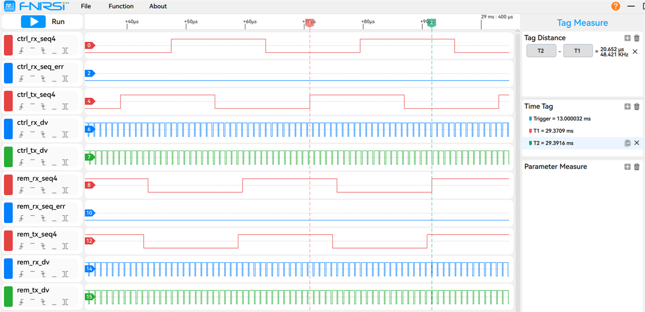
(above) Continuous 1MHz rate control messages, the ..seq4 signal inside the messages is high for 16 and then low for 16 messages. This allows us to see the system latency which is measured in the top right as Tag Distance = 20.652us. I promised the customer 2.47us so this is a problem !!
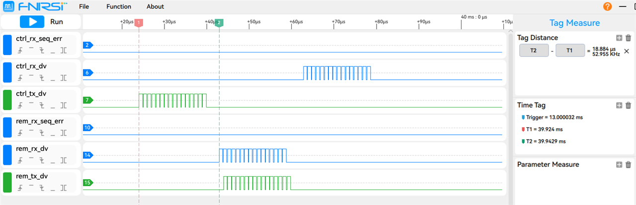
(above) Bursts of 16 x 1MHz rate control messages sent every 256us. The latency from ctrl_tx_valid to rem_rx_valid is a little different at 18.884 us. The only extra delay apart from the two PHYs (tx and rx) and the wire (1m = 4ns max) is the GMII to RGMII converter in the FPGA and there is no reason to believe that this could delay more than a few ns.
I discussed this issue with Claude who thought it would be worth turning the IEEE 802.3az Energy Efficient Ethernet (EEE) in the PHY. This requires an MDIO interface which wasn’t coded into the FPGA at the time, so I tried a different test which was very revealing.
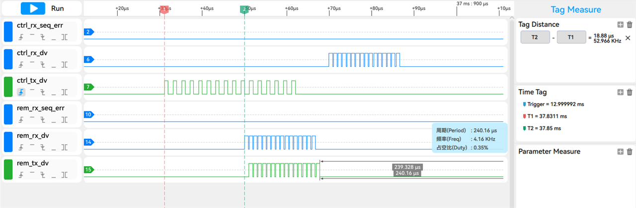
(above) Bursts of 16 x 500kHz rate control messages sent every 256us. This is unexpected ! The ctrl_tx_dv signal shows the messages being transmitted at the 500kHz rate but the rem_rx_dv signal shows that are output from the receiving PHY at a much higher rate. The PHY obviously DOES contain a buffer !
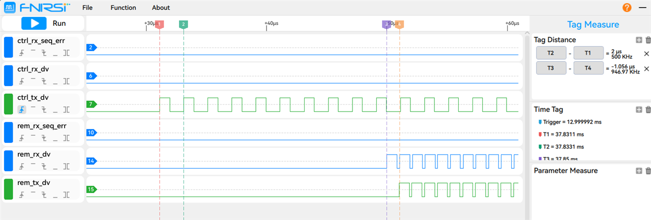
(above) Bursts of 16 x 500kHz rate control messages sent every 256us.
Here you clearly see the tx frame rate is 500kHz (2us period) and the rx_frame rate is 946.97kHz (1.056us period).
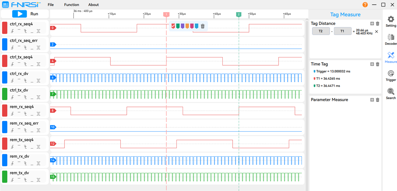
(above) Bursts of 16 x 500kHz rate control messages sent every 256us.
Latency measured between seq4 frame contents is exactly the same at 500kHz frame rate as it was at 1MHz.
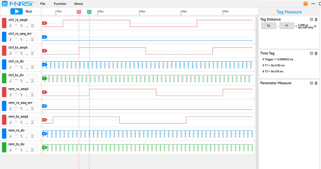
(above) Continuous 1MHz rate control messages, the ..seq4 signal inside the messages is high for 16 and then low for 16 messages. But now the Energy Efficient Ethernet is turned off. This takes some odd fiddling with the PHY internal registers via the MDIO interface (the default is that EEE is enabled). But now the PHY does work the way you might expect and the measured Latency between the transmitted and received frame data is right where it ought to be at 2.488us. Most of this comes from the logic in the FPGA.
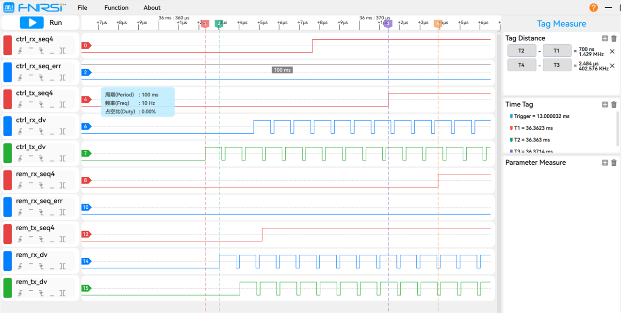
(above) Continuous 1MHz rate control messages, EEE turned off. The delay between tx_dv and rx_dv is down to 700ns – which about what one would expect from a GMII to RGMII converter, 2 PHYs, 1M of cable and an RGMII interface.
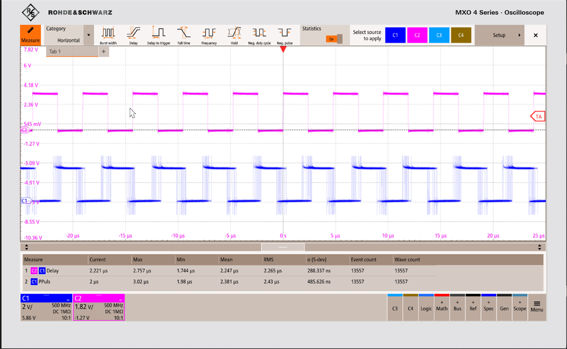
(above) Top trace: 200kHz square wave from signal generator applied to an input pin on the Remote. Lower trace: Corresponding output pin on Control. The jitter is to be expected because the signal generator is not synchronised to the 1MHz data frame timing. The mean delay is 2.247us which is within spec (and very slightly less than the delay timed by sequence content for reasons that are deterministic but too complicated to explain in this blog !)
Conclusions
All too often we just accept what ‘s offered because it’s the standard thing that just works - but if you put the effort in then a custom solution can do a lot more. The standard GB Ethernet approach with typical software drivers and MAC and PHY at standard settings, will get you significantly less data throughput, 10x (at least) worse latency and an easier life. There are other choices.
The adventurous approach would be helped if so many manufacturers wouldn’t try to hide their data sheets ! Standards bodies don’t help either : the official price for the EEE 802.3az Energy Efficient Ethernet (EEE) standard is $528.
I found the use of AI helpful in this work. I used Claude for advice ,and it works pretty well but neither Claude nor Google AI seemed to really understand the detail of the latency problem. I found nothing about it by searching in a more conventional way either (until after I had fixed it) – so I hope this Blog may be helpful to someone.
Turning off the Energy Efficient Ethernet in other system might improve performance - and although measuring it was not the purpose of my testing - it doesn't look as if EEE being on saves very much, if any, power in a heavily loaded system.
Comments and questions welcome.
MK
-

JWx
-
Cancel
-
Vote Up
0
Vote Down
-
-
Sign in to reply
-
More
-
Cancel
-

michaelkellett
in reply to JWx
-
Cancel
-
Vote Up
0
Vote Down
-
-
Sign in to reply
-
More
-
Cancel
-

JWx
in reply to michaelkellett
-
Cancel
-
Vote Up
0
Vote Down
-
-
Sign in to reply
-
More
-
Cancel
-

JWx
in reply to JWx
-
Cancel
-
Vote Up
0
Vote Down
-
-
Sign in to reply
-
More
-
Cancel
-

michaelkellett
in reply to JWx
-
Cancel
-
Vote Up
0
Vote Down
-
-
Sign in to reply
-
More
-
Cancel
Comment-

michaelkellett
in reply to JWx
-
Cancel
-
Vote Up
0
Vote Down
-
-
Sign in to reply
-
More
-
Cancel
Children