 Blond Moment
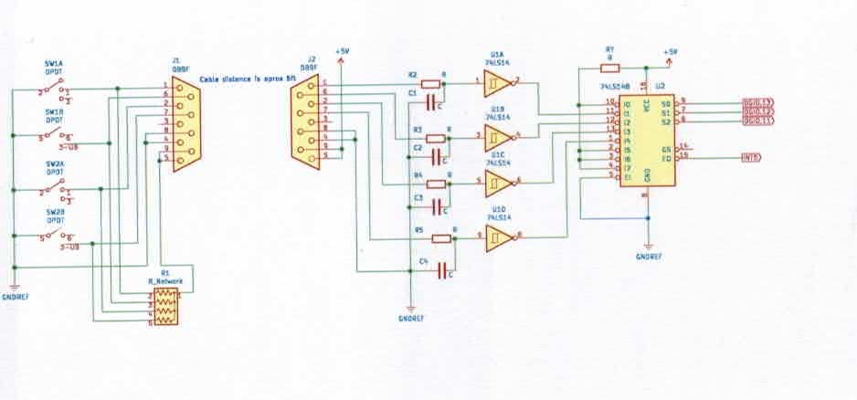
Ok, Boy Blond Moment Strikes Again: if you remember I used a CANbus Module hooked up via an I2C bus. But Wait nope it's the SPI bus. And the 2 switches in my diagram showed them hooked up to Digital Pins directly, even though they will have to be debounced with a Schmitt Trigger and an R/C network before they get to the CPU. Now back to the silliness of 'Who's on First'. I need to prioritize which of the five (5) states the switches are in. If I take the output of the two switches and send the 4 lines to the input of a priority encoder, this gives me 000, 001, 010, 011, and 100 as outputs plus I also get GS as well. E0 which is low when one of the inputs goes low. To prevent an output in the zero state, the 0 input pin is pulled up via 5v. Now E0 will only go low during a low, which goes to an interrupt pin on the processor. BTW, please don't ask me why I did not use software debouncing. It just eats CPU time, and I don't like to waste it.
Below I have included an abbreviated Function Table for a 74xx148, and a schematic of the switches and the logic for them. I used ![]() to do the schematic and the custom switch.
to do the schematic and the custom switch.
|
Abbreviated Function Table 74xx148
|
  |
|||||||||||||||||||||||||||||||||||||||||||||||||||||||||||||||||||||||||||||||||
Here is an UPDATED Wiring Plan.
| Wiring Plan | ||||||||
|---|---|---|---|---|---|---|---|---|
| Arduino Mega | IO Modules | Arduino Leonardo | Instrument Head | |||||
| mnemonic | pin | mnemonic | pin | mnemonic | pin | mnemonic | pin | |
| SI | ICSP.10 | SI | ||||||
| SO | ICSP.11 | SO | ||||||
| SCK | ICSP.9 | SCK | ||||||
| DIO.0.x | 13 | CS | ||||||
| INT1 | 2 | INT | ||||||
| DP | 12 | RST1 | ||||||
| DP | 11 | RST2 | ||||||
| DP | 10 | CE1 | ||||||
| DP | 9 | CE2 | ||||||
| DP | 8 | CLK1 | ||||||
| DP | 7 | CLK2 | ||||||
| DP | 6 | RD1 | ||||||
| DP | 5 | RD2 | ||||||
| DIO.I.13 | 13 | See Logic Diagram | FILL | J1.1 | ||||
| DIO.I.12 | 12 | See Logic Diagram | TEST | J1.6 | ||||
| DIO.I.11 | 11 | See Logic Diagram | UP | J1.2 | ||||
| INT5 | 21 | See Logic Diagram | DOWN | J1.7 | ||||
| VCC | VCC | VCC | ||||||
| GND | GND | GND | ||||||
| RS232 | ||||||||
| TX1 | 18 | RX | 0 | |||||
| RX1 | 19 | TX | 1 | |||||
| VCC | VCC | |||||||
| GND | GND | |||||||
| RS232 | ||||||||
| TX | TX | |||||||
| RX | RX | |||||||
| VCC | VCC | |||||||
| GND | GND | |||||||
| I2C - CAN Module | ||||||||
| INT5 | INT | J1.1 | ||||||
| SCK | SCK | J1.2 | ||||||
| SI | SI | J1.3 | ||||||
| SO | SO | J1.4 | ||||||
| DIO.O.x | CS | J1.5 | ||||||
| GND | GND | J1.6 | ||||||
| VCC | VCC | J1.7 | ||||||
Notes:
- I will be adding and or changing pin numbers as I go along.
- I will add the values for the RC circuit. TDB
Updates:
- 1/1/23: I surrounded the 74xx148 table and the logic Diagram with a table to get them to look correct.
- 1/1/23: I took out 6 <br> between the new table and the Wiring Plan Table.
- 1/1/23: I had to add one line in the Wiring Plan to include SCK - SCK which goes to the MC23017 from the Laerdeno the line has been underlined.
- 1/1/23: I am getting the SI, SO, SCK from the ICSP connector.
- 11/4/23: Can't even spell blond.. LOL
- 11/4/23: Added why I don't like software debouncing.
Parts List:
| Ref | Description | Part Number | Manufacture | Quantity |
|---|---|---|---|---|
| S1 | Switch-Supplied DPDT-centerOFF | 8856K12 | 1 | |
| S2 | Switch-Supplied DPDT-centerOFF | 8869K11X | 1 | |
| J1,2 | Connector, DB9 Female Crimp | L177RRE09SVF | ||
| Pins | Pins, Crimp for D-sub connectors | 16 | ||
| R1 | Resistor Pack | |||
| R2, 3, 4, 5 | Resistor* | |||
| R6 | Resistor | |||
| C1, 2, 3, 4* | Capacitor |
