


Well it looks like I found a working 5 volt supply that works!  It's a Lambda LXS-A-5-0V (a brick, and this is stock photo off the web).. So I wanted to test the the power supply. So I grabbed the Fuel Load Indicator, that I tore apart in my blog post NexGen: Hacking the Fuel Load Indicator.
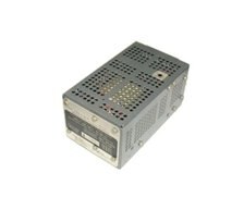
I hooked my +5 to pin 16 of the display and Ground on pin 17 and I got the following:
| Manufacturer: | LAMBDA | |
| Model Number: | LXS-A-5-0V | |
| Output Voltage: | 0 - 5 vdc | |
| Output Current: | 4 amps | |
Upon Power Up I got a "No Data" message (Figure 2)
Depressing the right hand switch to the test position (Figure 3) then (Figure 4) and then back to (Figure 1)
So at least I now have a starting point using an arduino.
The header from the display board is a 15x2 or 30 pin header ( 0.10" x 0.10" centers)
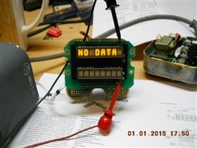 | 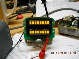 | 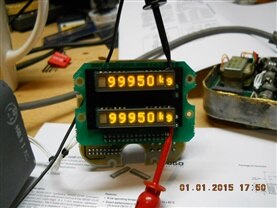 |
| Figure 2 "No Data" Message | Figure 3 Self Test I | Figure 4 Self Test Message II |
This is what I will need to run the displays:
- 8 data lines
- 5 Address Lines
- 7 Control Lines ( CLS, CLK, WR, RD, CE, FL*, RST )
- This is 19 20 pins + 5 more for the switches
- 24 25 pins Total
Note: FL* This pin is for accessing flash ram and will not be used.
Here is a link to a similar project http://www.nycresistor.com/2010/05/30/working-with-the-hdsp-2111/. The big difference between the hdsp-2111 and my hdsp-2131 is that the 2111 is a plastic part and my part is a hirel glass sealed over ceramic. Both, the 2111 and the 2131 share the same I/O; so a lot of my work is done. But they are using a Arduino Diecimila and I plan on using a Arduino Meg 2560 which has much more I/O pins which means I would not have to use the shift register. Also my two (2) hdsp-2131 displays are already mounted on a PCB that I will not modify. The hdsp display series data bus is bidirectional.
| Mnemonic | U1 | U2 | J1 | |
|---|---|---|---|---|
| Power | ||||
| Vcc | 16 | + | 16 | 28, 30 |
| GND | 17 | + | 17 | 3 |
| Logic GND | 18 | + | 18 | 4 |
| Data Bus | ||||
| D0 | 11 | + | 11 | 5 |
| D1 | 12 | + | 12 | 8 |
| D2 | 13 | + | 13 | 10 |
| D3 | 14 | + | 14 | 7 |
| D4 | 19 | + | 19 | 2 |
| D5 | 20 | + | 20 | 6 |
| D6 | 21 | + | 21 | 1 |
| D7 | 22 | 22 | 24[U1] 22[U2] | |
| Address Bus | ||||
| A0 | 28 | + | 28 | 11 |
| A1 | 29 | + | 29 | 9 |
| A2 | 30 | + | 30 | 12 |
| A3 | 31 | + | 31 | 27, 29 |
| A4 | 32 | + | 32 | 27, 29 |
| Controls | ||||
| CLS | 1 | 1 | 14[U1] 15[U2] | |
| CLK | 2 | 2 | 23[U1] 21[U2] | |
| WR | 3 | + | 3 | 16 |
| CE | 4 | 4 | 20[U1] 17[U2] | |
| RST | 5 | 5 | 25[U1] 26[U2] | |
| RD | 6 | 6 | 19[U1] 18[U2] | |
| FL | 27 | 27 | 13 |
The two way of showing this data, firs is laid out buy looking at the pins of J1.
The other way of showing this data by grouping functions together by their mnemonic.
| Mnemonic | J1 pins | To | To | To |
|---|---|---|---|---|
| D6 | 1 | U1-21 | U2-21 | |
| D4 | 2 | U1-19 | U2-19 | |
| GND display | 3 | U1-17 | U2-17 | |
| GND logic | 4 | U1-18 | U2-18 | |
| D0 | 5 | U1-11 | U2-11 | |
| D5 | 6 | U1-20 | U2-20 | |
| D3 | 7 | U1-14 | U2-14 | |
| D1 | 8 | U1-12 | U2-12 | |
| A1 | 9 | U1-29 | U2-29 | |
| D2 | 10 | U1-13 | U2-13 | |
| A0 | 11 | U1-28 | U2-28 | |
| A2 | 12 | U1-30 | U2-30 | |
| FL - Not Used | 13 | U1-27 | U2-27 | |
| CLS.1 | 14 | U1-1 | ||
| CLS.2 | 15 | U2-1 | ||
| WR | 16 | U1-23 | U2-3 | |
| CE.2 | 17 | U2-4 | ||
| RD.2 - Not Used | 18 | U2-6 | ||
| RD.1 - Not Used | 19 | U1-6 | ||
| CE.1 | 20 | U1-4 | ||
| D7.2 | 22 | U2-22 | ||
| CLK.2 | 21 | U2-2 | ||
| CLK.1 | 23 | U1-2 | ||
| D7.1 | 24 | U1-22 | ||
| RST.1 | 25 | U1-5 | ||
| RST.2 | 26 | U2-5 | ||
| A3 & A4 | 27 | U1-31 | U2-31 | 29 |
| Vcc | 28 | U1-16 | U2-16 | 30 |
| A3 & A4 | 29 | U1-32 | U2-32 | 27 |
| Vcc | 30 | U1-16 | U2-16 | 28 |
Keep Tuned In, More To Come
~~Cris 
BTW: It seems I can't add in the above list;
8 + 5 + 7 = 20 != 19
There for the next number should be 25 Total
~~Cris  6/4/15
Top Comments
-

DAB
-
Cancel
-
Vote Up
+1
Vote Down
-
-
Sign in to reply
-
More
-
Cancel
Comment-

DAB
-
Cancel
-
Vote Up
+1
Vote Down
-
-
Sign in to reply
-
More
-
Cancel
Children