


1. Introduction
First of all I would like to start with an apology to those who started following this series early on, I appreciate that it's been a while since I have published any articles in this series, and for this I am sorry, but I will be publishing much more regularly from now on.
I've been getting a few queries on how to create various packages both here and elsewhere, so I thought I would post up an additional example of creating a package in EAGLE based on the latest query I have received. This morning I had a question from rflmota asking for a bit more info on how I would go about creating custom shapes and he asked about a specific example for a POWERSO-36 used by the STM L6470 motor driver.
Ricardo conveniently supplied the package drawing for the part which I have shown below and we will use this for the basis of creating this package.
The full package details are available from ST in a detailed application note detailing the use of their high power packages: AN668 APPLICATION NOTE
So without further ado, lets get on with turning the above drawing into an EAGLE package!
2. Creating POWERSO-36 Package
2.1. Setting up the grids
We can see from the above that the pitch of the main 36 pins is 0.65mm or 0.025in. We can also see that the centre to centre pitch between the rows is 15.465mm - 1.7mm = 13.765mm. So we'll set our initial grid settings to 0.325 for the main grid and 6.8825 for the alt grids.
GRID MM 0.325 ON; GRID ALT MM 6.8825;
Later, once we've placed the initial pins and moved them to where they should be with respect to the origin we'll change the grid again for creating the central pad shape. For this we'll start with a main grid of 0.5mm to draw the basic shape and then reconfigure the grid as needed to get the shape to the correct size.
2.2. Placing the pads
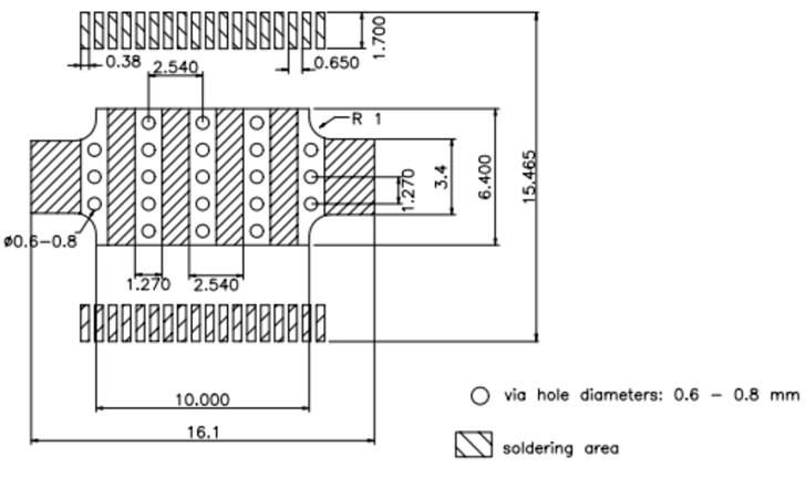
We'll start with the 36 main pads along each side of the device. For the purposes of this exercise we will assume that the default stop mask and solder paste aperture generation provides adequate results for these 36 pads. If not then follow the previous blog article where I show how to draw these layers manually and then copy/paste as appropriate to create the required pins. For this example, these pads are 0.38mm x 1.7mm in size so we start by issuing the following command:
SMD 0.38MMX1.7MM '1'
We can go and place the first row of 18 pads for one half of the package centralised horizontally and vertically on the origin. Then we group these and move them using the ALT grid to move them downwards by 6.8825mm. Using the GROUP and MOVE commands we now create the second row, based on the first row but 6.8825mm above the origin rather than below. Ensure that the orientation of this second row is correct such that the pin numbering correctly flows around the package as per the devices data sheet. Once you have done this the package will look like the following:
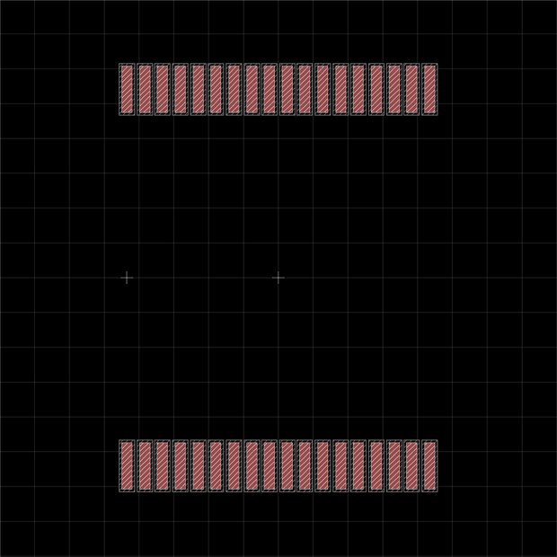
It's time to add in the basis for the central pad. The added polygon has to completely surround this so we'll make it smaller than the polygon. In this case we'll set it to be the region of the intersection of the horizontal and vertical so 10mm by 3.4mm and we don't want automatic generation of thermal relief, stop mask or solder paste apertures.
SMD 10MMX3.4MM NOTHERMALS NOSTOP NOCREAM 'PAD'
Click to place this pad on the origin.
Now you have placed this it's time to move on and draw the custom shaped polygon. At this point the package will look like the following:

2.3. Drawing the custom pad shape
For this section we need to change the grid to enable us to draw the the outline correctly. We'll use a main grid of 0.5mm which will give us adequate resolution to draw the correct contours and we'll use a 0.05mm grid to allow accurate adjustments to correct positioning afterwards.
GRID MM 0.5 ON; GRID ALT MM 0.05;
We can start drawing the custom polygon shape by on the top layer by issuing the following command.
LAYER Top; POLYGON
We'll work clockwise around the device clicking points around until we've draw the correct shape. During this we'll need to change the bend style to select the curved bend style and switch between them accordingly depending on the direction needed. Click on the icon the the toolbar at the top to switch to the radius bend style.
Click at the following co-ordinates to draw the outline of the polygon and complete by double clicking the final point back on the same starting point. The points required to draw the initial outline are:
(-5.0 -3.0) (-5.0 -2.5) (-6.0 -1.5) (-8.0 -1.5) (-8.0 1.5) (-6.0 1.5) (-5.0 2.5) (-5.0 3.0) (5.0 3.0) (5.0 2.5) (6.0 1.5) (8.0 1.5) (8.0 -1.5) (6.0 -1.5) (5.0 -2.5) (5.0 -3.0) (-5.0 -3.0) (-5.0 -3.0)
At for each of the curved sections (i.e. where the X and Y values both change) keep an eye on the direction of the bend and change the bend style between 5 and 6 accordingly. You can do this with Cmd+Right Click (Ctrl on Windows/Linux) or if you are using v8.3.2 or earlier just click on the bend style in the toolbar. Do not cancel the polygon command.
We have the basic outline but it's not quite right. Firstly we drew it on a grid which didn't give the precise positioning we need to make it easy to draw quickly by eye and secondly we haven't factored in the line width of the polygon and corrected for that. Using the ALT grid move the left and right hand edged to -8.05mm and 8.05mm respectively. Now group everything in the bottom half of the polygon and group move it using the ALT grid to it is sat on -3.2mm. Repeat the same for the top half so it is sat at 3.2mm.
Finally to correct for the line width we need to set the grid to half the currently set line width. In my case the line with is 0.127mm so I have set my grid to 0.0635mm. Now I work my way round the polygon and move each line (not individual points) exactly 1 grid space inwards. In doing this the curves will end up with the 1mm radius being correctly on the outer edge.
Once you have done this you will have a package which looks like the following:
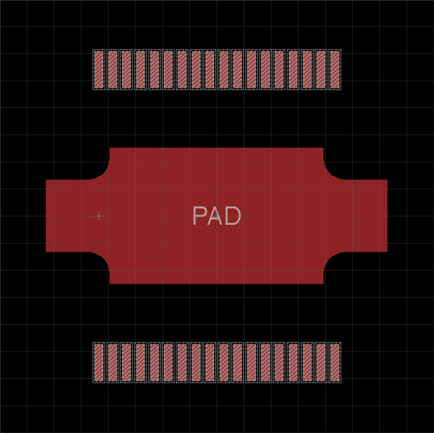
2.4. Drawing the solder mask and paste mask
The package drawing isn't 100% clear on the solder mask and paste mask apertures so I am going to make some assumptions here. Firstly they sit exactly on the outline of the main pad and secondly that the two end sections are exactly covering the rectangular end sections and the four middle sections are 1.27mm wide. Now we can go ahead and use the polygon command and the above techniques again to draw the areas identified by the hashing as "Soldering Area" on both the tStop and tCream layers. I won't go into the details on this as it's pretty much a repeat of the above several times over but with less complex polygons.
First of all I will set the grid up then I will go ahead and draw the polygons. I'll firstly draw them on the tStop layer and then I will go ahead and group copy them and put them onto the tCream layer too.
For the outer two areas a grid of 0.5mm and an alt grid of 0.05mm will allow these to be drawn correctly.
GRID MM 0.5 ON; GRID ALT 0.05;
Once these two outer polygons are drawn on tStop we can reset the grid to draw the remaining four.
GRID MM 1.27 ON; GRID ALT 0.0635; POLYGON
I've set the ALT grid so I can subtly alter the sizes of all these polygons after the initial drawing to mitigate the errors caused by the line width the same as I did above for the main copper polygon on the top layer. Once you've completed it you should see a package which looks like the following:
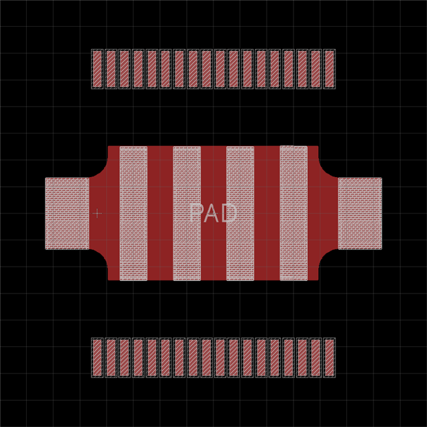
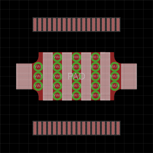
2.5. Adding thermal vias
There are two ways to do this. You can add through hole pads with the appropriate drill diameter to the package and ensure they are all mapped correctly to the same GND pin of the symbol or alternatively you can add vias in the layout. I prefer to add vias in the layout as it gives flexibility in the layout. I'll go ahead and add them as pads in the package here to illustrate how it's done.
I'll set the pad diameter to 1.27mm so it's the width of the gaps between the mask aperture openings and I will set the drill size to 0.8mm as specified in the data sheet.
CHANGE DRILL 0.8MM; PAD 1.27MM ROUND NOSTOP NOTHERMALS 'VIA1'
After adding the vias in the locations shown in the package drawing your package should be as follows:
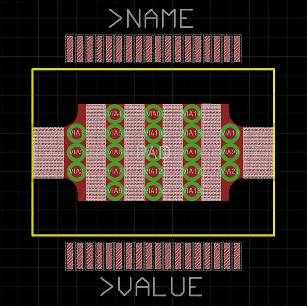
2.6. Creating the Silkscreen and Assembly Drawing Content
Finally we need to draw the package body outline on tPlace and on tDocu so that it appears on the silkscreen and the assembly drawings and also the >NAME and >VALUE text on tNames and tValues respectively. After drawing these the resulting package will look like the following:
3. The Completed POWERSO-36 Package
The following video shows how I quickly created this package based on the above specifications.
>>>> I'LL INSERT THE VIDEO HERE ONCE I HAVE FINISHED EDITING IT
This concludes the addendum to the fourth part of my new EAGLE tutorial series. Let me know what you think in the comments below and if you have any questions please feel free to ask!
Top Comments