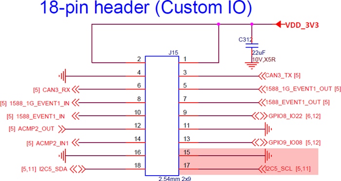
Attention: the J15 (the "other" header) pinout description in AVNET Guidelines is WRONG!
Flip pin 15 and 17:
pin 15 is GND
pin 17 is I2C5_SCL
These pins (J15, p17 = SCL and J15, pin 18 = SDA) have a 2K2 pull-up on board
and they are shared with the onboard I2S DAC (for audio out):
check which I2C Slave Address is occupied (used, by the onboard DAC) when connecting
other I2C slaves on I2C5.

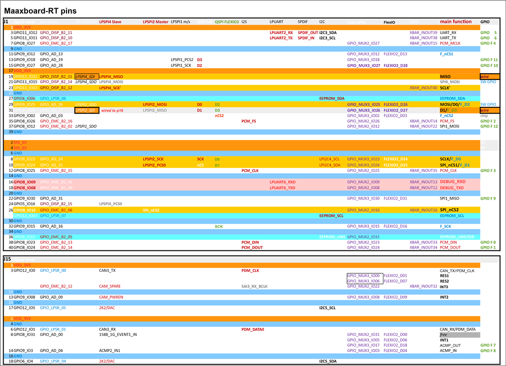
Figure 1: here correct MaaxBoard-RT J15 pinout


