Hello,
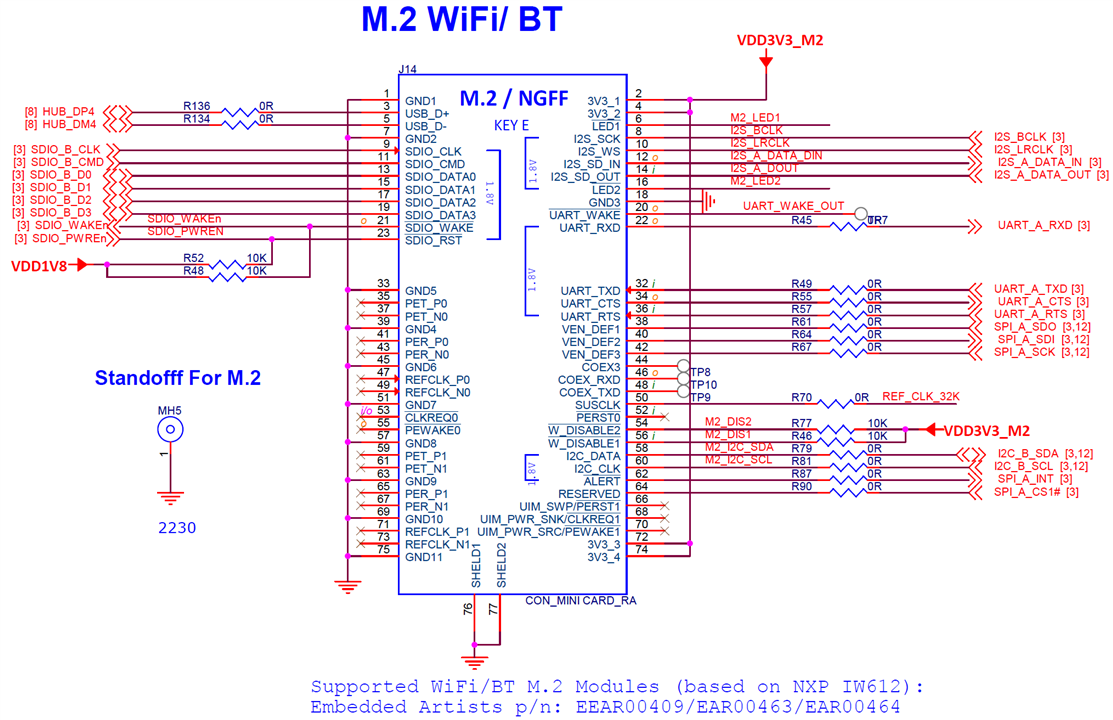
after reading documentation and hardware user guides for MaaXBoard OSM93 it is still unclear to me how the pins from M.2 connector (J14) are mapped to the OSM93 module.
Are there anywhere more details than this diagram from the hardware user guide?
Especially information about the GPIOs is completely missing.
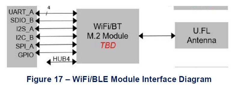
I also found out that the Block Diagram (Figure 7 in the Hardware User Guide) shows a differen SDIO interface than the one actually used.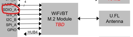
Best regards,
Werner