element14 Community
element14 Community
    Register Log In
  • Site
  • Search
  • Log In Register
  • About Us
  • Community Hub
    Community Hub
    • What's New on element14
    • Feedback and Support
    • Benefits of Membership
    • Personal Blogs
    • Members Area
    • Achievement Levels
  • Learn
    Learn
    • Ask an Expert
    • eBooks
    • element14 presents
    • Learning Center
    • Tech Spotlight
    • STEM Academy
    • Webinars, Training and Events
    • Learning Groups
  • Technologies
    Technologies
    • 3D Printing
    • FPGA
    • Industrial Automation
    • Internet of Things
    • Power & Energy
    • Sensors
    • Technology Groups
  • Challenges & Projects
    Challenges & Projects
    • Design Challenges
    • element14 presents Projects
    • Project14
    • Arduino Projects
    • Raspberry Pi Projects
    • Project Groups
  • Products
    Products
    • Arduino
    • Avnet Boards Community
    • Dev Tools
    • Manufacturers
    • Multicomp Pro
    • Product Groups
    • Raspberry Pi
    • RoadTests & Reviews
  • Store
    Store
    • Visit Your Store
    • Choose another store...
      • Europe
      •  Austria (German)
      •  Belgium (Dutch, French)
      •  Bulgaria (Bulgarian)
      •  Czech Republic (Czech)
      •  Denmark (Danish)
      •  Estonia (Estonian)
      •  Finland (Finnish)
      •  France (French)
      •  Germany (German)
      •  Hungary (Hungarian)
      •  Ireland
      •  Israel
      •  Italy (Italian)
      •  Latvia (Latvian)
      •  
      •  Lithuania (Lithuanian)
      •  Netherlands (Dutch)
      •  Norway (Norwegian)
      •  Poland (Polish)
      •  Portugal (Portuguese)
      •  Romania (Romanian)
      •  Russia (Russian)
      •  Slovakia (Slovak)
      •  Slovenia (Slovenian)
      •  Spain (Spanish)
      •  Sweden (Swedish)
      •  Switzerland(German, French)
      •  Turkey (Turkish)
      •  United Kingdom
      • Asia Pacific
      •  Australia
      •  China
      •  Hong Kong
      •  India
      •  Korea (Korean)
      •  Malaysia
      •  New Zealand
      •  Philippines
      •  Singapore
      •  Taiwan
      •  Thailand (Thai)
      • Americas
      •  Brazil (Portuguese)
      •  Canada
      •  Mexico (Spanish)
      •  United States
      Can't find the country/region you're looking for? Visit our export site or find a local distributor.
  • Translate
  • Profile
  • Settings
Avnet Boards Forums
  • Products
  • Dev Tools
  • Avnet Boards Community
  • Avnet Boards Forums
  • More
  • Cancel
Avnet Boards Forums
ZedBoard Hardware Design audio passthrough using SPI in PL
  • Forum
  • Documents
  • Members
  • Mentions
  • Sub-Groups
  • Tags
  • More
  • Cancel
  • New
Join Avnet Boards Forums to participate - click to join for free!
Actions
  • Share
  • More
  • Cancel
Forum Thread Details
  • State Not Answered
  • Replies 7 replies
  • Subscribers 321 subscribers
  • Views 673 views
  • Users 0 members are here
Related

audio passthrough using SPI in PL

Former Member
Former Member 8 months ago

Hi!

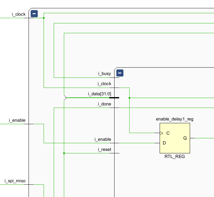
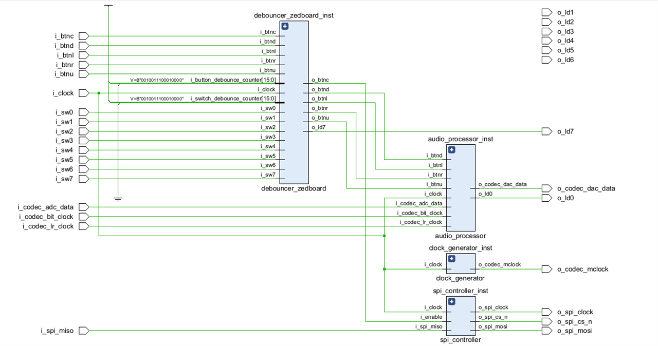
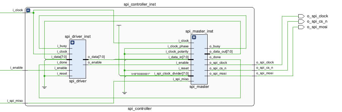
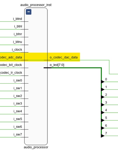
I'm new to FPGA and ZedBoard, and for educational purpose, I'm trying to recive signal from microphone(or LINE_IN) and passthrough it to headphones(or LINE_OUT). Eventually I'm going to create a sound recognition system(frequency detection to be precisie), but for now, I want to properly set up audio codec, and check on headphones if I can hear myself. I found interesting project here: https://www.rtlaudiolab.com/page/4/ (part1-5) that describes how to passtrough audio using SPI communication. I set up everything, just like on this website, but have a problem with SPI driver(which is the codec audio if I understand that correctly), because the data_in are going nowhere. I don't know if that's how it supossed to be, but common sense tell me that it shouldn't  be that way. Also, I can generate a bitstream and program zedboard, but i can't hear nothing.

I would be thankful for any advice and help.

PS. Acording to website of the project, i should press BTNC before i could hear anything but that doesn;t help either.

Here are screenshots from the vivado:

imageimage

  • Sign in to reply
  • Cancel
Parents
  • jc2048
    0 jc2048 8 months ago

    Qualification: I don't use Vivado and don't own a Zedboard, so this is just in very general terms.

    The audio data streams in to the FPGA on the i_codec_(xxx) inputs.

    Given the names, it's most likely the CODEC chip has an I2S output. Serial data on adc_data, clock on bit_clock, and the left-right qualifier on lr_clock.

    It's possible that the CODEC being used here has a register set that needs to be loaded via SPI at the start (sometimes they're I2C, sometimes SPI, and sometimes there's no setup and it's just done by strapping inputs on the CODEC chip). Normally that would be done from a processor, but can also be done from logic (it's usually quite a small selection of options, so not too onerous). Try going down a level into the spi_controller_inst and see if there's not only a shift register for the SPI, but also a simple state machine to sequence everything and a store of the values that will be sent in sequence to the CODEC.

    If that's the case, the i_spi_miso input would come from the CODEC, for reading back register contents, but may not actually be necessary to get the CODEC set up (there's a good chance it could work just by pushing the right data at it).

    Hopefully that will get you a bit further.

    • Cancel
    • Vote Up 0 Vote Down
    • Sign in to reply
    • Verify Answer
    • Cancel
  • Former Member
    0 Former Member 8 months ago in reply to jc2048

    Yeah, I should've said that earlier. The audio codec on zedboard is ADAU1761. The I2C is default, and for set up SPI, in spi_driver_inst there are 3 dummies write sends to spi_master. Also in documentation of that codec was said so. As i told before, I'm new to FPGA, and i dont understand everything that has been written in that intances, and I'm not sure why there's need to configure SPI eventually, because I only need the audio output to use further in PL. Could you help me understand that? My job for now is to short the LINE_IN and LINE_OUT to make sure that board is working properly.

    Also, in audio_proccessor_inst there are simple assign o_codec_dac_data to i_codec adc_data. Is that could work, or something is missing?. Of course the name of that pins are from constraints file dedicated to this zedboard.

    • Cancel
    • Vote Up 0 Vote Down
    • Sign in to reply
    • Verify Answer
    • Cancel
  • michaelkellett
    0 michaelkellett 8 months ago in reply to Former Member

    I'm seriously puzzled by your diagram.

    The SPI controller does not appear to have any reset or parallel data input/output - how does it know what config data to send out, when to send it etc etc.

    If you want to accept analogue input data on the ADC input to the codec and output analogue data on its audio output DAC you will need to initialise the codec, then the FPGA can accept serial digital data from the codec ADC and buffer it , read from the buffer and output serial digital data to the codec which will use its DAC to convert it to analogue audio data.

    I'm not sure that you have got the hang of how to clock the codec and the FPGA, the LR clock from the codec will be synchronous with the M clock into the codec. It is unlikely that you will run the FPGA synchronously with the LR clock and you may well have a choice between clocking data out of the codec synchronously with M clock of FPGA clock. There will be timing constraints in the codec spec about clocking and the MUST be observed if you want it to work correctly.

    I suggest that you find a complete working example of a pass through application for your hardware and study it carefully. Then try tweaking it a bit. I took a quick look at the example you linked and although I didn't like its use of video rather than static diagrams it probably covers a lot of what you need. Have you been able to make it work ?

    MK

    • Cancel
    • Vote Up 0 Vote Down
    • Sign in to reply
    • Verify Answer
    • Cancel
Reply
  • michaelkellett
    0 michaelkellett 8 months ago in reply to Former Member

    I'm seriously puzzled by your diagram.

    The SPI controller does not appear to have any reset or parallel data input/output - how does it know what config data to send out, when to send it etc etc.

    If you want to accept analogue input data on the ADC input to the codec and output analogue data on its audio output DAC you will need to initialise the codec, then the FPGA can accept serial digital data from the codec ADC and buffer it , read from the buffer and output serial digital data to the codec which will use its DAC to convert it to analogue audio data.

    I'm not sure that you have got the hang of how to clock the codec and the FPGA, the LR clock from the codec will be synchronous with the M clock into the codec. It is unlikely that you will run the FPGA synchronously with the LR clock and you may well have a choice between clocking data out of the codec synchronously with M clock of FPGA clock. There will be timing constraints in the codec spec about clocking and the MUST be observed if you want it to work correctly.

    I suggest that you find a complete working example of a pass through application for your hardware and study it carefully. Then try tweaking it a bit. I took a quick look at the example you linked and although I didn't like its use of video rather than static diagrams it probably covers a lot of what you need. Have you been able to make it work ?

    MK

    • Cancel
    • Vote Up 0 Vote Down
    • Sign in to reply
    • Verify Answer
    • Cancel
Children
  • Former Member
    0 Former Member 8 months ago in reply to michaelkellett

    Hey, I read the documentation of the audio codec, and i get it that to set up the SPI communication i have to pull ~CLATCH 3 times low, and it is written in spi_driver. I also understand that those other "messages" have to be sent, to properly work, but in that implementation, i dont understand what is going on in spi_master, especially that half of the code includes clock_phase and  clock_polarity that are grounded.  If you or anyone could look at the example here: https://www.rtlaudiolab.com/004-zedboard-audio-codec-spi-controller/ and tell me if thats correct i would be thankful.

    Also, i dont understand why i_spi_miso get involved here, cause the whole spi_controller has only sending the configuration to o_spi_mosi, so why we have the reading option here. Below i'm putting screenshot of whole spi_controller for the record.

    About that clock that you mentioned, the i_codec_lr_clock and bit_clock are nowhere used. The clock generator are "creating" 45MHz clock that is send to mclock, in that project was said that if I want to sampling in 44.1kHz, the mclock should be 1024xfs, in documentation i found it too(in the case of not using internal PLL).

    About the example, unfortunately I didn't found another example of setting audio codec with SPI using only PL. It's not that I can't use it, just prefer to use PL if thats possible.

    image

    • Cancel
    • Vote Up 0 Vote Down
    • Sign in to reply
    • Verify Answer
    • Cancel
  • michaelkellett
    0 michaelkellett 8 months ago in reply to Former Member

    I can't review the code in your link because its written in Verilog which I can understand but never use if I can help it. So I am not confident in spotting bugs in Verilog code.

    Having said that, there is a bug in the spi_controller block diagram which casts huge doubt on the utility of the whole rtaudio project as a learning aid.

    i_reset input to the spi_master block is grounded, if you look at the code for the spi_master block you will see that all this should happen when reset is asserted:

            if (i_reset) begin
                fsm_state <= IDLE;
                spi_data_counter <= \'b0;
                spi_cs_n <= 1\'b1;
                data_out_shift <= \'b0;
                done <= 1\'b0;
                spi_mosi <= 1\'b0;
                data_out_shift <= \'b0;
                o_data_out <= \'b0;
                o_busy <= \'b0;
    

    It is possible that the complete project will work, or often work depending on the way the registers start up, but not certain. To fail to initialise a standard block like the SPI in this way, is  what I would call an unforgivable error. It is a deliberate action (not an error of omission) which will result in an uncertain design. To do this in a published teaching style project is beyond sloppy ! Do NOT trust this project .

    Moving on ........

    The SPI_MASTER is a standard block of code (the audiolab article says:

    "The SPI Master is a generic module that implements the master device in a single-slave SPI bus. In addition to the standard SPI signals, the clock phase and polarity of the SPI Master can be changed at runtime using the corresponding input ports. The bit width of a transaction can be adjusted during the module instantiation." )

    Using standard blocks of code is common but, as in this case, frequently results in features in the code that are not required for your specific application. SPI is  a bidirectional protocol, but you only need on direction so some unwanted connections are to be expected. You have a miso pin but you don't need it.

    In section 5 of the rtaudio project they have a block diagram of the audio pass through:

    image

    This is a bit of it and you can see that they connect the codec_adc_data output directly to the codec dac_data input. This is a trivial and pointless audio pass through application in which the data is never read properly into the FPGA and the bit clock and LR clock rely on internal synchronisation in the codec chip. It will tell you if the codec is working but not that you can actually read and write digitised data from/to it.

    The do cover this later:

    image

    I have not checked their code at all !

    (If you have considered using VHDL then let me know - I could then provide some code examples (but not for your hardware, although obviously modifiable.)

    MK

    • Cancel
    • Vote Up 0 Vote Down
    • Sign in to reply
    • Verify Answer
    • Cancel
  • Former Member
    0 Former Member 8 months ago in reply to michaelkellett

    Hey, thanks for your effort. I really appreciate that. I found that earlier, and even assign it for another button, but it doesnt help either. I wanted to simply check the audio codec, if it's working properly. I won't be sending any signal to audio output further in the project. What I need is having digitilized signal on known "port", to further analisys. But for now, I have struggle with audio codec :(

    I have a question about that master module, especially abaout that part that you mentioned, and the few lines under that. If I'm correct, I could simply start the procedure of configurating codec after reset? With that, I would have one button to reset and start sending messages.

    Also, if you could explain in your own words what exactly is bit clock and LR clock, and about that internal synchronisation. I will be very grateful.

    • Cancel
    • Vote Up 0 Vote Down
    • Sign in to reply
    • Verify Answer
    • Cancel
  • michaelkellett
    0 michaelkellett 8 months ago in reply to Former Member

    The spi_drive code is suspect because it doesn't use reset and the state machine may start up in any state.

    Pressing the enable button should kick things off - you shouldn't need to auto start the driver writing to the codec registers but if those missing resets are spoiling things it won't work.

    It's normal when working on FPGA code to simulate before running on actual hardware. It will help you understand what is going on much better if you can get into that habit.

    If you don't have access to a simulator you should sort that out first - it is a necessary tool.

    You could modify the spi driver to toggle spare output pins as it does certain things so you can see if it is working.

    Or connect a scope to the SPI mosi output to the codec and look for the *** config. signals.

    The data sheet for the ADAU1761explains the timing of all signals very well - you need to study that document carefully.

    MK

    • Cancel
    • Vote Up 0 Vote Down
    • Sign in to reply
    • Verify Answer
    • Cancel
element14 Community

element14 is the first online community specifically for engineers. Connect with your peers and get expert answers to your questions.

  • Members
  • Learn
  • Technologies
  • Challenges & Projects
  • Products
  • Store
  • About Us
  • Feedback & Support
  • FAQs
  • Terms of Use
  • Privacy Policy
  • Legal and Copyright Notices
  • Sitemap
  • Cookies

An Avnet Company © 2025 Premier Farnell Limited. All Rights Reserved.

Premier Farnell Ltd, registered in England and Wales (no 00876412), registered office: Farnell House, Forge Lane, Leeds LS12 2NE.

ICP 备案号 10220084.

Follow element14

  • X
  • Facebook
  • linkedin
  • YouTube