

Hello!
We are currently working on a project which requires us to extend a previously created memory interface on a ZedBoard from being 4k in size to 256k (A 1/4 of a MB).
We had previously created a file, called pocket_core_top_mem.v which instantiated a 4k long memory (4 xilinx_tdpram_1024x36 modules) that has been working for the longest time. This old interface used only 4 blocks of 140 available Block RAM modules on the zedboard for the project (50 blocks are used elsewhere, leaving 86 remaining).
// Memory I/O for pocket_core_top

module pocket_core_top_mem
  (
  input              clk_bist,          // BIST clock
  input              reset_bist,   	    // Sync active high reset

  input              clk_axi,           // Clock for AXI4 domain
  input              reset_axi,         // Active high sync reset
  input wire         tdp_en_a,          // Enable operations RAM Port A
  input wire         tdp_en_b,          // Enable operations RAM Port B
  input wire [3:0]   tdp_wren_a,        // Write Enables RAM Port A
  input wire [11:0]  tdp_addr_a,        // Address RAM Port A
  input wire [11:0]  tdp_addr_b,        // Address RAM Port B
  input wire [31:0]  tdp_din_a,         // Write Data RAM Port A
  input wire [31:0]  tdp_din_b,         // Write Data RAM Port B
  output wire [31:0] tdp_dout_a,        // Read Data RAM Port A
  output wire [31:0] tdp_dout_b			// Read Data RAM Port B
  );

// TDP Clk & Rst Port A
wire tdp_clk_a   = clk_axi;
wire tdp_reset_a = reset_axi;


// TDP Clk & Rst Port B
wire tdp_clk_b   = clk_bist;
wire tdp_reset_b = reset_bist;
wire [3:0] tdp_wren_b = {4{tdp_en_b}};

// TDP Byte Enable Port A
wire tdp_en_a_0 = tdp_en_a & ~tdp_addr_a[11] & ~tdp_addr_a[10];
wire tdp_en_a_1 = tdp_en_a & ~tdp_addr_a[11] &  tdp_addr_a[10];
wire tdp_en_a_2 = tdp_en_a &  tdp_addr_a[11] & ~tdp_addr_a[10];
wire tdp_en_a_3 = tdp_en_a &  tdp_addr_a[11] &  tdp_addr_a[10];

// TDP Byte Enable Port B
wire tdp_en_b_0 = tdp_en_b & ~tdp_addr_b[11] & ~tdp_addr_b[10];
wire tdp_en_b_1 = tdp_en_b & ~tdp_addr_b[11] &  tdp_addr_b[10];
wire tdp_en_b_2 = tdp_en_b &  tdp_addr_b[11] & ~tdp_addr_b[10];
wire tdp_en_b_3 = tdp_en_b &  tdp_addr_b[11] &  tdp_addr_b[10];

// Write Data RAM Port A
wire [35:0] int_tdp_din_a = {4'd0, tdp_din_a[31:0]};

// Write Data RAM Port B
wire [35:0] int_tdp_din_b = {4'd0, tdp_din_b[31:0]};

// Single Module Read Data RAM Port A
wire [35:0] int_tdp_dout_a_0;
wire [35:0] int_tdp_dout_a_1;
wire [35:0] int_tdp_dout_a_2;
wire [35:0] int_tdp_dout_a_3;

// Single Module Read Data RAM Port B
wire [35:0] int_tdp_dout_b_0;
wire [35:0] int_tdp_dout_b_1;
wire [35:0] int_tdp_dout_b_2;
wire [35:0] int_tdp_dout_b_3;

// Read Data RAM Port A
wire [35:0] int_tdp_dout_a = tdp_addr_a[11] ?
							(tdp_addr_a[10] ? int_tdp_dout_a_3 : int_tdp_dout_a_2 ) :
							(tdp_addr_a[10] ? int_tdp_dout_a_1 : int_tdp_dout_a_0 ) ;

// Read Data RAM Port B
wire [35:0] int_tdp_dout_b = tdp_addr_b[11] ?
							(tdp_addr_b[10] ? int_tdp_dout_b_3 : int_tdp_dout_b_2 ) :
							(tdp_addr_b[10] ? int_tdp_dout_b_1 : int_tdp_dout_b_0 ) ;


// Assign Outputs
assign tdp_dout_a[31:0] = int_tdp_dout_a[31:0];
assign tdp_dout_b[31:0] = int_tdp_dout_b[31:0];


xilinx_tdpram_1024x36 RAM_I_0 (
   .clk_a   (tdp_clk_a)        // input         Clock Port A
  ,.reset_a (tdp_reset_a)      // input         Sync active high reset
  ,.en_a    (tdp_en_a_0)       // input         Enable operations Port A
  ,.regce_a (1'b0)             // input         Output Register Clock Enable Port A - Not using OutReg
  ,.wren_a  (tdp_wren_a[3:0])  // input   [3:0] Write Enables Port A
  ,.addr_a  (tdp_addr_a[9:0])  // input   [9:0] Address Port A
  ,.din_a   (int_tdp_din_a[35:0])  // input  [35:0] Data Port A
  ,.dout_a  (int_tdp_dout_a_0[35:0]) // output [35:0] Data Port A

  ,.clk_b   (tdp_clk_b)        // input         Clock Port B
  ,.reset_b (tdp_reset_b)  	   // input         Sync active high reset
  ,.en_b    (tdp_en_b_0)       // input         Enable operations Port B
  ,.regce_b (1'b0)             // input         Output Register Clock Enable Port B
  ,.wren_b  (tdp_wren_b[3:0])  // input   [3:0] Write Enables Port B
  ,.addr_b  (tdp_addr_b[9:0])  // input   [9:0] Address Port B
  ,.din_b   (int_tdp_din_b[35:0])  // input  [35:0] Data Port B
  ,.dout_b  (int_tdp_dout_b_0[35:0]) // output [35:0] Data Port B
);

xilinx_tdpram_1024x36 RAM_I_1 (
   .clk_a   (tdp_clk_a)        // input         Clock Port A
  ,.reset_a (tdp_reset_a)      // input         Sync active high reset
  ,.en_a    (tdp_en_a_1)       // input         Enable operations Port A
  ,.regce_a (1'b0)             // input         Output Register Clock Enable Port A - Not using OutReg
  ,.wren_a  (tdp_wren_a[3:0])  // input   [3:0] Write Enables Port A
  ,.addr_a  (tdp_addr_a[9:0])  // input   [9:0] Address Port A
  ,.din_a   (int_tdp_din_a[35:0])  // input  [35:0] Data Port A
  ,.dout_a  (int_tdp_dout_a_1[35:0]) // output [35:0] Data Port A

  ,.clk_b   (tdp_clk_b)        // input         Clock Port B
  ,.reset_b (tdp_reset_b)  	   // input         Sync active high reset
  ,.en_b    (tdp_en_b_1)       // input         Enable operations Port B
  ,.regce_b (1'b0)             // input         Output Register Clock Enable Port B
  ,.wren_b  (tdp_wren_b[3:0])  // input   [3:0] Write Enables Port B
  ,.addr_b  (tdp_addr_b[9:0])  // input   [9:0] Address Port B
  ,.din_b   (int_tdp_din_b[35:0])  // input  [35:0] Data Port B
  ,.dout_b  (int_tdp_dout_b_1[35:0]) // output [35:0] Data Port B
);

xilinx_tdpram_1024x36 RAM_I_2 (
   .clk_a   (tdp_clk_a)        // input         Clock Port A
  ,.reset_a (tdp_reset_a)      // input         Sync active high reset
  ,.en_a    (tdp_en_a_2)       // input         Enable operations Port A
  ,.regce_a (1'b0)             // input         Output Register Clock Enable Port A - Not using OutReg
  ,.wren_a  (tdp_wren_a[3:0])  // input   [3:0] Write Enables Port A
  ,.addr_a  (tdp_addr_a[9:0])  // input   [9:0] Address Port A
  ,.din_a   (int_tdp_din_a[35:0])  // input  [35:0] Data Port A
  ,.dout_a  (int_tdp_dout_a_2[35:0]) // output [35:0] Data Port A

  ,.clk_b   (tdp_clk_b)        // input         Clock Port B
  ,.reset_b (tdp_reset_b)  	   // input         Sync active high reset
  ,.en_b    (tdp_en_b_2)       // input         Enable operations Port B
  ,.regce_b (1'b0)             // input         Output Register Clock Enable Port B
  ,.wren_b  (tdp_wren_b[3:0])  // input   [3:0] Write Enables Port B
  ,.addr_b  (tdp_addr_b[9:0])  // input   [9:0] Address Port B
  ,.din_b   (int_tdp_din_b[35:0])  // input  [35:0] Data Port B
  ,.dout_b  (int_tdp_dout_b_2[35:0]) // output [35:0] Data Port B
);

xilinx_tdpram_1024x36 RAM_I_3 (
   .clk_a   (tdp_clk_a)        // input         Clock Port A
  ,.reset_a (tdp_reset_a)      // input         Sync active high reset
  ,.en_a    (tdp_en_a_3)       // input         Enable operations Port A
  ,.regce_a (1'b0)             // input         Output Register Clock Enable Port A - Not using OutReg
  ,.wren_a  (tdp_wren_a[3:0])  // input   [3:0] Write Enables Port A
  ,.addr_a  (tdp_addr_a[9:0])  // input   [9:0] Address Port A
  ,.din_a   (int_tdp_din_a[35:0])  // input  [35:0] Data Port A
  ,.dout_a  (int_tdp_dout_a_3[35:0]) // output [35:0] Data Port A

  ,.clk_b   (tdp_clk_b)        // input         Clock Port B
  ,.reset_b (tdp_reset_b)      // input         Sync active high reset
  ,.en_b    (tdp_en_b_3)       // input         Enable operations Port B
  ,.regce_b (1'b0)             // input         Output Register Clock Enable Port B
  ,.wren_b  (tdp_wren_b[3:0])  // input   [3:0] Write Enables Port B
  ,.addr_b  (tdp_addr_b[9:0])  // input   [9:0] Address Port B
  ,.din_b   (int_tdp_din_b[35:0])  // input  [35:0] Data Port B
  ,.dout_b  (int_tdp_dout_b_3[35:0]) // output [35:0] Data Port B
);


endmodule // pocket_core_top_mem
While doing this, we simply started by trying to nest multiple memory files (using xilinx_tdpram_1024x36 modules), where we would have a .v file and module for 16k ram (4 4k modules), a file for 64k ram (4 16k modules), and finally a top file which consisted of 4 64k modules. (called pocket_core_mem_16k.v, pocket_core_mem_64k.v, and pocket_core_top_mem_nested.v here).
// Memory I/O for pocket_core_mem_16k

module pocket_core_mem_16k
  (
  input              rx_clk,          // BIST clock
  input              reset_bist,   	    // Sync active high reset

  input              clk_axi,           // Clock for AXI4 domain
  input              reset_axi,         // Active high sync reset
  input wire         tdp_en_a,          // Enable operations RAM Port A
  input wire         tdp_en_b,          // Enable operations RAM Port B
  input wire [3:0]   tdp_wren_a,        // Write Enables RAM Port A
  input wire [11:0]  tdp_addr_a,        // Address RAM Port A
  input wire [11:0]  tdp_addr_b,        // Address RAM Port B
  input wire [31:0]  tdp_din_a,         // Write Data RAM Port A
  input wire [31:0]  tdp_din_b,         // Write Data RAM Port B
  output wire [31:0] tdp_dout_a,        // Read Data RAM Port A
  output wire [31:0] tdp_dout_b			// Read Data RAM Port B
  );

// TDP Clk & Rst Port A
wire tdp_clk_a   = clk_axi;
wire tdp_reset_a = reset_axi;


// TDP Clk & Rst Port B
wire tdp_clk_b   = rx_clk;
wire tdp_reset_b = reset_bist;
wire [3:0] tdp_wren_b = {4{tdp_en_b}};

// RAM Select MUX Signal
reg [1:0] ram_sel_a = 2'b00;
reg [1:0] ram_sel_b = 2'b00;

// TDP Byte Enable Port A
wire tdp_en_a_0 = tdp_en_a & ~tdp_addr_a[11] & ~tdp_addr_a[10];
wire tdp_en_a_1 = tdp_en_a & ~tdp_addr_a[11] &  tdp_addr_a[10];
wire tdp_en_a_2 = tdp_en_a &  tdp_addr_a[11] & ~tdp_addr_a[10];
wire tdp_en_a_3 = tdp_en_a &  tdp_addr_a[11] &  tdp_addr_a[10];

// TDP Byte Enable Port B
wire tdp_en_b_0 = tdp_en_b & ~tdp_addr_b[11] & ~tdp_addr_b[10];
wire tdp_en_b_1 = tdp_en_b & ~tdp_addr_b[11] &  tdp_addr_b[10];
wire tdp_en_b_2 = tdp_en_b &  tdp_addr_b[11] & ~tdp_addr_b[10];
wire tdp_en_b_3 = tdp_en_b &  tdp_addr_b[11] &  tdp_addr_b[10];

// Write Data RAM Port A
wire [35:0] int_tdp_din_a = {4'd0, tdp_din_a[31:0]};

// Write Data RAM Port B
wire [35:0] int_tdp_din_b = {4'd0, tdp_din_b[31:0]};

// Single Module Read Data RAM Port A
wire [35:0] int_tdp_dout_a_0;
wire [35:0] int_tdp_dout_a_1;
wire [35:0] int_tdp_dout_a_2;
wire [35:0] int_tdp_dout_a_3;

// Single Module Read Data RAM Port B
wire [35:0] int_tdp_dout_b_0;
wire [35:0] int_tdp_dout_b_1;
wire [35:0] int_tdp_dout_b_2;
wire [35:0] int_tdp_dout_b_3;

// Read Data RAM Port A
wire [35:0] int_tdp_dout_a = ram_sel_a[1] ?
							(ram_sel_a[0] ? int_tdp_dout_a_3 : int_tdp_dout_a_2 ) :
							(ram_sel_a[0] ? int_tdp_dout_a_1 : int_tdp_dout_a_0 ) ;

// Read Data RAM Port B
wire [35:0] int_tdp_dout_b = ram_sel_b[1] ?
							(ram_sel_b[0] ? int_tdp_dout_b_3 : int_tdp_dout_b_2 ) :
							(ram_sel_b[0] ? int_tdp_dout_b_1 : int_tdp_dout_b_0 ) ;


// Assign Outputs
assign tdp_dout_a[31:0] = int_tdp_dout_a[31:0];
assign tdp_dout_b[31:0] = int_tdp_dout_b[31:0];


xilinx_tdpram_1024x36 RAM_I_0 (
   .clk_a   (tdp_clk_a)        // input         Clock Port A
  ,.reset_a (tdp_reset_a)      // input         Sync active high reset
  ,.en_a    (tdp_en_a_0)       // input         Enable operations Port A
  ,.regce_a (1'b0)             // input         Output Register Clock Enable Port A - Not using OutReg
  ,.wren_a  (tdp_wren_a[3:0])  // input   [3:0] Write Enables Port A
  ,.addr_a  (tdp_addr_a[9:0])  // input   [9:0] Address Port A
  ,.din_a   (int_tdp_din_a[35:0])  // input  [35:0] Data Port A
  ,.dout_a  (int_tdp_dout_a_0[35:0]) // output [35:0] Data Port A

  ,.clk_b   (tdp_clk_b)        // input         Clock Port B
  ,.reset_b (tdp_reset_b)  	   // input         Sync active high reset
  ,.en_b    (tdp_en_b_0)       // input         Enable operations Port B
  ,.regce_b (1'b0)             // input         Output Register Clock Enable Port B
  ,.wren_b  (tdp_wren_b[3:0])  // input   [3:0] Write Enables Port B
  ,.addr_b  (tdp_addr_b[9:0])  // input   [9:0] Address Port B
  ,.din_b   (int_tdp_din_b[35:0])  // input  [35:0] Data Port B
  ,.dout_b  (int_tdp_dout_b_0[35:0]) // output [35:0] Data Port B
);

xilinx_tdpram_1024x36 RAM_I_1 (
   .clk_a   (tdp_clk_a)        // input         Clock Port A
  ,.reset_a (tdp_reset_a)      // input         Sync active high reset
  ,.en_a    (tdp_en_a_1)       // input         Enable operations Port A
  ,.regce_a (1'b0)             // input         Output Register Clock Enable Port A - Not using OutReg
  ,.wren_a  (tdp_wren_a[3:0])  // input   [3:0] Write Enables Port A
  ,.addr_a  (tdp_addr_a[9:0])  // input   [9:0] Address Port A
  ,.din_a   (int_tdp_din_a[35:0])  // input  [35:0] Data Port A
  ,.dout_a  (int_tdp_dout_a_1[35:0]) // output [35:0] Data Port A

  ,.clk_b   (tdp_clk_b)        // input         Clock Port B
  ,.reset_b (tdp_reset_b)  	   // input         Sync active high reset
  ,.en_b    (tdp_en_b_1)       // input         Enable operations Port B
  ,.regce_b (1'b0)             // input         Output Register Clock Enable Port B
  ,.wren_b  (tdp_wren_b[3:0])  // input   [3:0] Write Enables Port B
  ,.addr_b  (tdp_addr_b[9:0])  // input   [9:0] Address Port B
  ,.din_b   (int_tdp_din_b[35:0])  // input  [35:0] Data Port B
  ,.dout_b  (int_tdp_dout_b_1[35:0]) // output [35:0] Data Port B
);

xilinx_tdpram_1024x36 RAM_I_2 (
   .clk_a   (tdp_clk_a)        // input         Clock Port A
  ,.reset_a (tdp_reset_a)      // input         Sync active high reset
  ,.en_a    (tdp_en_a_2)       // input         Enable operations Port A
  ,.regce_a (1'b0)             // input         Output Register Clock Enable Port A - Not using OutReg
  ,.wren_a  (tdp_wren_a[3:0])  // input   [3:0] Write Enables Port A
  ,.addr_a  (tdp_addr_a[9:0])  // input   [9:0] Address Port A
  ,.din_a   (int_tdp_din_a[35:0])  // input  [35:0] Data Port A
  ,.dout_a  (int_tdp_dout_a_2[35:0]) // output [35:0] Data Port A

  ,.clk_b   (tdp_clk_b)        // input         Clock Port B
  ,.reset_b (tdp_reset_b)  	   // input         Sync active high reset
  ,.en_b    (tdp_en_b_2)       // input         Enable operations Port B
  ,.regce_b (1'b0)             // input         Output Register Clock Enable Port B
  ,.wren_b  (tdp_wren_b[3:0])  // input   [3:0] Write Enables Port B
  ,.addr_b  (tdp_addr_b[9:0])  // input   [9:0] Address Port B
  ,.din_b   (int_tdp_din_b[35:0])  // input  [35:0] Data Port B
  ,.dout_b  (int_tdp_dout_b_2[35:0]) // output [35:0] Data Port B
);

xilinx_tdpram_1024x36 RAM_I_3 (
   .clk_a   (tdp_clk_a)        // input         Clock Port A
  ,.reset_a (tdp_reset_a)      // input         Sync active high reset
  ,.en_a    (tdp_en_a_3)       // input         Enable operations Port A
  ,.regce_a (1'b0)             // input         Output Register Clock Enable Port A - Not using OutReg
  ,.wren_a  (tdp_wren_a[3:0])  // input   [3:0] Write Enables Port A
  ,.addr_a  (tdp_addr_a[9:0])  // input   [9:0] Address Port A
  ,.din_a   (int_tdp_din_a[35:0])  // input  [35:0] Data Port A
  ,.dout_a  (int_tdp_dout_a_3[35:0]) // output [35:0] Data Port A

  ,.clk_b   (tdp_clk_b)        // input         Clock Port B
  ,.reset_b (tdp_reset_b)      // input         Sync active high reset
  ,.en_b    (tdp_en_b_3)       // input         Enable operations Port B
  ,.regce_b (1'b0)             // input         Output Register Clock Enable Port B
  ,.wren_b  (tdp_wren_b[3:0])  // input   [3:0] Write Enables Port B
  ,.addr_b  (tdp_addr_b[9:0])  // input   [9:0] Address Port B
  ,.din_b   (int_tdp_din_b[35:0])  // input  [35:0] Data Port B
  ,.dout_b  (int_tdp_dout_b_3[35:0]) // output [35:0] Data Port B
);


always @(posedge tdp_clk_a)
  begin
    if(tdp_reset_a)
      begin
        ram_sel_a[1:0] <= 2'b00;
      end
    else if(tdp_en_a)
      begin
        ram_sel_a[1:0] <= tdp_addr_a[11:10];
      end
  end

always @(posedge tdp_clk_b)
  begin
    if(tdp_reset_b)
      begin
        ram_sel_b[1:0] <= 2'b00;
      end
    else if(tdp_en_b)
      begin
        ram_sel_b[1:0] <= tdp_addr_b[11:10];
      end
  end


endmodule // pocket_core_mem_16k
// Memory I/O for pocket_core_mem_64k

module pocket_core_mem_64k
  (
  input              rx_clk,            // BIST clock
  input              reset_bist,   	    // Sync active high reset

  input              clk_axi,           // Clock for AXI4 domain
  input              reset_axi,         // Active high sync reset
  input wire         tdp_en_a,          // Enable operations RAM Port A
  input wire         tdp_en_b,          // Enable operations RAM Port B
  input wire [3:0]   tdp_wren_a,        // Write Enables RAM Port A
  input wire [13:0]  tdp_addr_a,        // Address RAM Port A
  input wire [13:0]  tdp_addr_b,        // Address RAM Port B
  input wire [31:0]  tdp_din_a,         // Write Data RAM Port A
  input wire [31:0]  tdp_din_b,         // Write Data RAM Port B
  output wire [31:0] tdp_dout_a,        // Read Data RAM Port A
  output wire [31:0] tdp_dout_b			// Read Data RAM Port B
  );

// TDP Clk & Rst Port A
wire tdp_clk_a   = clk_axi;
wire tdp_reset_a = reset_axi;

// TDP Clk & Rst Port B
wire tdp_clk_b   = rx_clk;
wire tdp_reset_b = reset_bist;

// RAM Select MUX Signal
reg [1:0] ram_sel_a = 2'b00;
reg [1:0] ram_sel_b = 2'b00;

// TDP Byte Enable Port A
wire tdp_en_a_0 = tdp_en_a & ~tdp_addr_a[13] & ~tdp_addr_a[12];
wire tdp_en_a_1 = tdp_en_a & ~tdp_addr_a[13] &  tdp_addr_a[12];
wire tdp_en_a_2 = tdp_en_a &  tdp_addr_a[13] & ~tdp_addr_a[12];
wire tdp_en_a_3 = tdp_en_a &  tdp_addr_a[13] &  tdp_addr_a[12];

// TDP Byte Enable Port B
wire tdp_en_b_0 = tdp_en_b & ~tdp_addr_b[13] & ~tdp_addr_b[12];
wire tdp_en_b_1 = tdp_en_b & ~tdp_addr_b[13] &  tdp_addr_b[12];
wire tdp_en_b_2 = tdp_en_b &  tdp_addr_b[13] & ~tdp_addr_b[12];
wire tdp_en_b_3 = tdp_en_b &  tdp_addr_b[13] &  tdp_addr_b[12];

// Write Data RAM Port A
//wire [35:0] int_tdp_din_a = {4'd0, tdp_din_a[31:0]};

// Write Data RAM Port B
//wire [35:0] int_tdp_din_b = {4'd0, tdp_din_b[31:0]};

// Single Module Read Data RAM Port A
wire [31:0] int_tdp_dout_a_0;
wire [31:0] int_tdp_dout_a_1;
wire [31:0] int_tdp_dout_a_2;
wire [31:0] int_tdp_dout_a_3;

// Single Module Read Data RAM Port B
wire [31:0] int_tdp_dout_b_0;
wire [31:0] int_tdp_dout_b_1;
wire [31:0] int_tdp_dout_b_2;
wire [31:0] int_tdp_dout_b_3;

// Read Data RAM Port A
wire [31:0] int_tdp_dout_a = ram_sel_a[1] ?
							(ram_sel_a[0] ? int_tdp_dout_a_3 : int_tdp_dout_a_2 ) :
							(ram_sel_a[0] ? int_tdp_dout_a_1 : int_tdp_dout_a_0 ) ;

// Read Data RAM Port B
wire [31:0] int_tdp_dout_b = ram_sel_b[1] ?
							(ram_sel_b[0] ? int_tdp_dout_b_3 : int_tdp_dout_b_2 ) :
							(ram_sel_b[0] ? int_tdp_dout_b_1 : int_tdp_dout_b_0 ) ;


// Assign Outputs
assign tdp_dout_a[31:0] = int_tdp_dout_a[31:0];
assign tdp_dout_b[31:0] = int_tdp_dout_b[31:0];


pocket_core_mem_16k RAM_16K_0 (
   .rx_clk      (tdp_clk_b)               // input         Clock Port B
  ,.reset_bist  (tdp_reset_b)             // input         Sync active high reset
  ,.clk_axi     (tdp_clk_a)               // input         Clock Port A
  ,.reset_axi   (tdp_reset_a)             // input         Sync active high reset

  ,.tdp_en_a    (tdp_en_a_0)              // input         Enable operations Port A
  ,.tdp_en_b    (tdp_en_b_0)              // input         Enable operations Port B
  ,.tdp_wren_a  (tdp_wren_a[3:0])         // input   [3:0] Write Enables Port A
  ,.tdp_addr_a  (tdp_addr_a[11:0])        // input  [11:0] Address Port A
  ,.tdp_addr_b  (tdp_addr_b[11:0])        // input  [11:0] Address Port B
  ,.tdp_din_a   (tdp_din_a[31:0])         // input  [31:0] Data Port A
  ,.tdp_din_b   (tdp_din_b[31:0])         // input  [31:0] Data Port B
  ,.tdp_dout_a  (int_tdp_dout_a_0[31:0])  // output [35:0] Data Port A
  ,.tdp_dout_b  (int_tdp_dout_b_0[31:0])  // output [35:0] Data Port B
);

pocket_core_mem_16k RAM_16K_1 (
   .rx_clk      (tdp_clk_b)               // input         Clock Port B
  ,.reset_bist  (tdp_reset_b)             // input         Sync active high reset
  ,.clk_axi     (tdp_clk_a)               // input         Clock Port A
  ,.reset_axi   (tdp_reset_a)             // input         Sync active high reset

  ,.tdp_en_a    (tdp_en_a_1)              // input         Enable operations Port A
  ,.tdp_en_b    (tdp_en_b_1)              // input         Enable operations Port B
  ,.tdp_wren_a  (tdp_wren_a[3:0])         // input   [3:0] Write Enables Port A
  ,.tdp_addr_a  (tdp_addr_a[11:0])        // input  [11:0] Address Port A
  ,.tdp_addr_b  (tdp_addr_b[11:0])        // input  [11:0] Address Port B
  ,.tdp_din_a   (tdp_din_a[31:0])         // input  [31:0] Data Port A
  ,.tdp_din_b   (tdp_din_b[31:0])         // input  [31:0] Data Port B
  ,.tdp_dout_a  (int_tdp_dout_a_1[31:0])  // output [31:0] Data Port A
  ,.tdp_dout_b  (int_tdp_dout_b_1[31:0])  // output [31:0] Data Port B
);

pocket_core_mem_16k RAM_16K_2 (
   .rx_clk      (tdp_clk_b)               // input         Clock Port B
  ,.reset_bist  (tdp_reset_b)             // input         Sync active high reset
  ,.clk_axi     (tdp_clk_a)               // input         Clock Port A
  ,.reset_axi   (tdp_reset_a)             // input         Sync active high reset

  ,.tdp_en_a    (tdp_en_a_2)              // input         Enable operations Port A
  ,.tdp_en_b    (tdp_en_b_2)              // input         Enable operations Port B
  ,.tdp_wren_a  (tdp_wren_a[3:0])         // input   [3:0] Write Enables Port A
  ,.tdp_addr_a  (tdp_addr_a[11:0])        // input  [11:0] Address Port A
  ,.tdp_addr_b  (tdp_addr_b[11:0])        // input  [11:0] Address Port B
  ,.tdp_din_a   (tdp_din_a[31:0])         // input  [31:0] Data Port A
  ,.tdp_din_b   (tdp_din_b[31:0])         // input  [31:0] Data Port B
  ,.tdp_dout_a  (int_tdp_dout_a_2[31:0])  // output [31:0] Data Port A
  ,.tdp_dout_b  (int_tdp_dout_b_2[31:0])  // output [31:0] Data Port B
);

pocket_core_mem_16k RAM_16K_3 (
   .rx_clk      (tdp_clk_b)               // input         Clock Port B
  ,.reset_bist  (tdp_reset_b)             // input         Sync active high reset
  ,.clk_axi     (tdp_clk_a)               // input         Clock Port A
  ,.reset_axi   (tdp_reset_a)             // input         Sync active high reset

  ,.tdp_en_a    (tdp_en_a_3)              // input         Enable operations Port A
  ,.tdp_en_b    (tdp_en_b_3)              // input         Enable operations Port B
  ,.tdp_wren_a  (tdp_wren_a[3:0])         // input   [3:0] Write Enables Port A
  ,.tdp_addr_a  (tdp_addr_a[11:0])        // input  [11:0] Address Port A
  ,.tdp_addr_b  (tdp_addr_b[11:0])        // input  [11:0] Address Port B
  ,.tdp_din_a   (tdp_din_a[31:0])         // input  [31:0] Data Port A
  ,.tdp_din_b   (tdp_din_b[31:0])         // input  [31:0] Data Port B
  ,.tdp_dout_a  (int_tdp_dout_a_3[31:0])  // output [31:0] Data Port A
  ,.tdp_dout_b  (int_tdp_dout_b_3[31:0])  // output [31:0] Data Port B
);

always @(posedge tdp_clk_a)
  begin
    if(tdp_reset_a)
      begin
        ram_sel_a[1:0] <= 2'b00;
      end
    else if(tdp_en_a)
      begin
        ram_sel_a[1:0] <= tdp_addr_a[13:12];
      end
  end

always @(posedge tdp_clk_b)
  begin
    if(tdp_reset_b)
      begin
        ram_sel_b[1:0] <= 2'b00;
      end
    else if(tdp_en_b)
      begin
        ram_sel_b[1:0] <= tdp_addr_b[13:12];
      end
  end

endmodule // pocket_core_mem_64k
// Memory I/O for pocket_core_top

module pocket_core_top_mem
  (
  input              rx_clk,          // BIST clock
  input              reset_bist,   	    // Sync active high reset

  input              clk_axi,           // Clock for AXI4 domain
  input              reset_axi,         // Active high sync reset
  input wire         tdp_en_a,          // Enable operations RAM Port A
  input wire         tdp_en_b,          // Enable operations RAM Port B
  input wire [3:0]   tdp_wren_a,        // Write Enables RAM Port A
  input wire [15:0]  tdp_addr_a,        // Address RAM Port A
  input wire [15:0]  tdp_addr_b,        // Address RAM Port B
  input wire [31:0]  tdp_din_a,         // Write Data RAM Port A
  input wire [31:0]  tdp_din_b,         // Write Data RAM Port B
  output wire [31:0] tdp_dout_a,        // Read Data RAM Port A
  output wire [31:0] tdp_dout_b			    // Read Data RAM Port B
  );

// TDP Clk & Rst Port A
wire tdp_clk_a   = clk_axi;
wire tdp_reset_a = reset_axi;

// RAM Select MUX Signal
reg [1:0] ram_sel_a = 2'b00;
reg [1:0] ram_sel_b = 2'b00;

// TDP Clk & Rst Port B
wire tdp_clk_b   = rx_clk;
wire tdp_reset_b = reset_bist;
//wire [3:0] tdp_wren_b = {4{tdp_en_b}};

// TDP Byte Enable Port A
wire tdp_en_a_0 = tdp_en_a & ~tdp_addr_a[15] & ~tdp_addr_a[14];
wire tdp_en_a_1 = tdp_en_a & ~tdp_addr_a[15] &  tdp_addr_a[14];
wire tdp_en_a_2 = tdp_en_a &  tdp_addr_a[15] & ~tdp_addr_a[14];
wire tdp_en_a_3 = tdp_en_a &  tdp_addr_a[15] &  tdp_addr_a[14];

// TDP Byte Enable Port B
wire tdp_en_b_0 = tdp_en_b & ~tdp_addr_b[15] & ~tdp_addr_b[14];
wire tdp_en_b_1 = tdp_en_b & ~tdp_addr_b[15] &  tdp_addr_b[14];
wire tdp_en_b_2 = tdp_en_b &  tdp_addr_b[15] & ~tdp_addr_b[14];
wire tdp_en_b_3 = tdp_en_b &  tdp_addr_b[15] &  tdp_addr_b[14];

// Write Data RAM Port A
//wire [35:0] int_tdp_din_a = {4'd0, tdp_din_a[31:0]};

// Write Data RAM Port B
//wire [35:0] int_tdp_din_b = {4'd0, tdp_din_b[31:0]};

// Single Module Read Data RAM Port A
wire [31:0] int_tdp_dout_a_0;
wire [31:0] int_tdp_dout_a_1;
wire [31:0] int_tdp_dout_a_2;
wire [31:0] int_tdp_dout_a_3;

// Single Module Read Data RAM Port B
wire [31:0] int_tdp_dout_b_0;
wire [31:0] int_tdp_dout_b_1;
wire [31:0] int_tdp_dout_b_2;
wire [31:0] int_tdp_dout_b_3;

// Read Data RAM Port A
wire [31:0] int_tdp_dout_a = ram_sel_a[1] ?
							(ram_sel_a[0] ? int_tdp_dout_a_3 : int_tdp_dout_a_2 ) :
							(ram_sel_a[0] ? int_tdp_dout_a_1 : int_tdp_dout_a_0 ) ;

// Read Data RAM Port B
wire [31:0] int_tdp_dout_b = ram_sel_b[1] ?
							(ram_sel_b[0] ? int_tdp_dout_b_3 : int_tdp_dout_b_2 ) :
							(ram_sel_b[0] ? int_tdp_dout_b_1 : int_tdp_dout_b_0 ) ;


// Assign Outputs
assign tdp_dout_a[31:0] = int_tdp_dout_a[31:0];
assign tdp_dout_b[31:0] = int_tdp_dout_b[31:0];


pocket_core_mem_64k RAM_64K_0 (
   .rx_clk      (tdp_clk_b)               // input         Clock Port B
  ,.reset_bist  (tdp_reset_b)             // input         Sync active high reset
  ,.clk_axi     (tdp_clk_a)               // input         Clock Port A
  ,.reset_axi   (tdp_reset_a)             // input         Sync active high reset

  ,.tdp_en_a    (tdp_en_a_0)              // input         Enable operations Port A
  ,.tdp_en_b    (tdp_en_b_0)              // input         Enable operations Port B
  ,.tdp_wren_a  (tdp_wren_a[3:0])         // input   [3:0] Write Enables Port A
  ,.tdp_addr_a  (tdp_addr_a[13:0])        // input  [13:0] Address Port A
  ,.tdp_addr_b  (tdp_addr_b[13:0])        // input  [13:0] Address Port B
  ,.tdp_din_a   (tdp_din_a[31:0])         // input  [31:0] Data Port A
  ,.tdp_din_b   (tdp_din_b[31:0])         // input  [31:0] Data Port B
  ,.tdp_dout_a  (int_tdp_dout_a_0[31:0])  // output [31:0] Data Port A
  ,.tdp_dout_b  (int_tdp_dout_b_0[31:0])  // output [31:0] Data Port B
);

pocket_core_mem_64k RAM_64K_1 (
   .rx_clk      (tdp_clk_b)               // input         Clock Port B
  ,.reset_bist  (tdp_reset_b)             // input         Sync active high reset
  ,.clk_axi     (tdp_clk_a)               // input         Clock Port A
  ,.reset_axi   (tdp_reset_a)             // input         Sync active high reset

  ,.tdp_en_a    (tdp_en_a_1)              // input         Enable operations Port A
  ,.tdp_en_b    (tdp_en_b_1)              // input         Enable operations Port B
  ,.tdp_wren_a  (tdp_wren_a[3:0])         // input   [3:0] Write Enables Port A
  ,.tdp_addr_a  (tdp_addr_a[13:0])        // input  [13:0] Address Port A
  ,.tdp_addr_b  (tdp_addr_b[13:0])        // input  [13:0] Address Port B
  ,.tdp_din_a   (tdp_din_a[31:0])         // input  [31:0] Data Port A
  ,.tdp_din_b   (tdp_din_b[31:0])         // input  [31:0] Data Port B
  ,.tdp_dout_a  (int_tdp_dout_a_1[31:0])  // output [31:0] Data Port A
  ,.tdp_dout_b  (int_tdp_dout_b_1[31:0])  // output [31:0] Data Port B
);

pocket_core_mem_64k RAM_64K_2 (
   .rx_clk      (tdp_clk_b)               // input         Clock Port B
  ,.reset_bist  (tdp_reset_b)             // input         Sync active high reset
  ,.clk_axi     (tdp_clk_a)               // input         Clock Port A
  ,.reset_axi   (tdp_reset_a)             // input         Sync active high reset

  ,.tdp_en_a    (tdp_en_a_2)              // input         Enable operations Port A
  ,.tdp_en_b    (tdp_en_b_2)              // input         Enable operations Port B
  ,.tdp_wren_a  (tdp_wren_a[3:0])         // input   [3:0] Write Enables Port A
  ,.tdp_addr_a  (tdp_addr_a[13:0])        // input  [13:0] Address Port A
  ,.tdp_addr_b  (tdp_addr_b[13:0])        // input  [13:0] Address Port B
  ,.tdp_din_a   (tdp_din_a[31:0])         // input  [31:0] Data Port A
  ,.tdp_din_b   (tdp_din_b[31:0])         // input  [31:0] Data Port B
  ,.tdp_dout_a  (int_tdp_dout_a_2[31:0])  // output [31:0] Data Port A
  ,.tdp_dout_b  (int_tdp_dout_b_2[31:0])  // output [31:0] Data Port B
);

pocket_core_mem_64k RAM_64K_3 (
   .rx_clk      (tdp_clk_b)               // input         Clock Port B
  ,.reset_bist  (tdp_reset_b)             // input         Sync active high reset
  ,.clk_axi     (tdp_clk_a)               // input         Clock Port A
  ,.reset_axi   (tdp_reset_a)             // input         Sync active high reset

  ,.tdp_en_a    (tdp_en_a_3)              // input         Enable operations Port A
  ,.tdp_en_b    (tdp_en_b_3)              // input         Enable operations Port B
  ,.tdp_wren_a  (tdp_wren_a[3:0])         // input   [3:0] Write Enables Port A
  ,.tdp_addr_a  (tdp_addr_a[13:0])        // input  [13:0] Address Port A
  ,.tdp_addr_b  (tdp_addr_b[13:0])        // input  [13:0] Address Port B
  ,.tdp_din_a   (tdp_din_a[31:0])         // input  [31:0] Data Port A
  ,.tdp_din_b   (tdp_din_b[31:0])         // input  [31:0] Data Port B
  ,.tdp_dout_a  (int_tdp_dout_a_3[31:0])  // output [31:0] Data Port A
  ,.tdp_dout_b  (int_tdp_dout_b_3[31:0])  // output [31:0] Data Port B
);

always @(posedge tdp_clk_a)
  begin
    if(tdp_reset_a)
      begin
        ram_sel_a[1:0] <= 2'b00;
      end
    else if(tdp_en_a)
      begin
        ram_sel_a[1:0] <= tdp_addr_a[15:14];
      end
  end

always @(posedge tdp_clk_b)
  begin
    if(tdp_reset_b)
      begin
        ram_sel_b[1:0] <= 2'b00;
      end
    else if(tdp_en_b)
      begin
        ram_sel_b[1:0] <= tdp_addr_b[15:14];
      end
  end

endmodule // pocket_core_top_mem
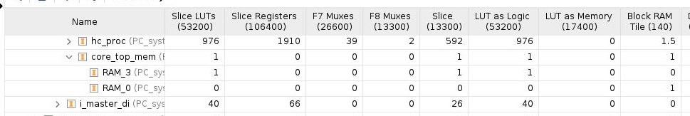
Unfortunately, when we went to build the project, it ran through with no errors and wrote the bitstream but unfortunately only 2 RAM blocks were instantiated in the implemented design and I was only able to read and write to 0x100 of the memory space I programmed in. In Vivado, it was only reporting that 51 of the 140 RAM blocks were instantiated.
So, I then created and ran a simulation in Icarus Verilog on my files to see if I could indeed read and write to the higher address blocks. This simulation worked and proved my files didn't have a design error.
I was dumbstruck and thought it was how Vivado interpreted my file methodology that was making the error occur. So, I then simply made a single file (named pocket_core_top_mem_single.v here) with 64 xilinx_tdpram_1024x36 modules in it.
This STILL only had 2 RAM blocks instantiated when Vivado finished building and writing the bitstream:
I also ran simulations to confirm if this file worked or not, and they confirmed the file worked.
pocket_core_top_mem_single.v.txt
Would there be anything that could be preventing Vivado from instantiating these 64 BRAM blocks that I may have missed?
Regards,
Daniel