

Hi,
I added IOBUFG component in the vivado and trying to connect the input to pin R1(from J1) and output to N4(From J6), during placement I'm facing error saying it can't be connected as there is no possibility to connect.
How can i drive the IOBUFG in vivado.
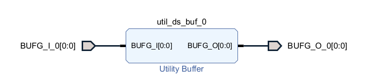
Below is my design.
My constraints are:
set_property PACKAGE_PIN N4 [get_ports BUFG_O_0]
set_property IOSTANDARD SSTL12 [get_ports BUFG_O_0]
set_property PACKAGE_PIN A8 [get_ports BUFG_I_0]
set_property IOSTANDARD LVCMOS18 [get_ports BUFG_I_0]
The error I'm facing is below:
[Place 30-675] Sub-optimal placement for a global clock-capable IO pin and BUFG pair.If this sub optimal condition is acceptable for this design, you may use the CLOCK_DEDICATED_ROUTE constraint in the .xdc file to demote this message to a WARNING. However, the use of this override is highly discouraged. These examples can be used directly in the .xdc file to override this clock rule. < set_property CLOCK_DEDICATED_ROUTE FALSE [get_nets BUFG_I_0_IBUF[0]_inst/O] > BUFG_I_0_IBUF[0]_inst/IBUFCTRL_INST (IBUFCTRL.O) is locked to IOB_X0Y32 design_1_i/util_ds_buf_0/U0/USE_BUFG.GEN_BUFG[0].BUFG_U (BUFGCE.I) is provisionally placed by clockplacer on BUFGCE_X0Y19 The above error could possibly be related to other connected instances. Following is a list of all the related clock rules and their respective instances. Clock Rule: rule_bufgce_bufg_conflict Status: PASS Rule Description: Only one of the 2 available sites (BUFGCE or BUFGCE_DIV/BUFGCTRL) in a pair can be used at the same time and design_1_i/util_ds_buf_0/U0/USE_BUFG.GEN_BUFG[0].BUFG_U (BUFGCE.O) is provisionally placed by clockplacer on BUFGCE_X0Y19
I would appreciate any suggestions.
Thanks,
Nirupama.T