element14 Community
element14 Community
    Register Log In
  • Site
  • Search
  • Log In Register
  • About Us
  • Community Hub
    Community Hub
    • What's New on element14
    • Feedback and Support
    • Benefits of Membership
    • Personal Blogs
    • Members Area
    • Achievement Levels
  • Learn
    Learn
    • Ask an Expert
    • eBooks
    • element14 presents
    • Learning Center
    • Tech Spotlight
    • STEM Academy
    • Webinars, Training and Events
    • Learning Groups
  • Technologies
    Technologies
    • 3D Printing
    • FPGA
    • Industrial Automation
    • Internet of Things
    • Power & Energy
    • Sensors
    • Technology Groups
  • Challenges & Projects
    Challenges & Projects
    • Design Challenges
    • element14 presents Projects
    • Project14
    • Arduino Projects
    • Raspberry Pi Projects
    • Project Groups
  • Products
    Products
    • Arduino
    • Avnet Boards Community
    • Dev Tools
    • Manufacturers
    • Multicomp Pro
    • Product Groups
    • Raspberry Pi
    • RoadTests & Reviews
  • Store
    Store
    • Visit Your Store
    • Choose another store...
      • Europe
      •  Austria (German)
      •  Belgium (Dutch, French)
      •  Bulgaria (Bulgarian)
      •  Czech Republic (Czech)
      •  Denmark (Danish)
      •  Estonia (Estonian)
      •  Finland (Finnish)
      •  France (French)
      •  Germany (German)
      •  Hungary (Hungarian)
      •  Ireland
      •  Israel
      •  Italy (Italian)
      •  Latvia (Latvian)
      •  
      •  Lithuania (Lithuanian)
      •  Netherlands (Dutch)
      •  Norway (Norwegian)
      •  Poland (Polish)
      •  Portugal (Portuguese)
      •  Romania (Romanian)
      •  Russia (Russian)
      •  Slovakia (Slovak)
      •  Slovenia (Slovenian)
      •  Spain (Spanish)
      •  Sweden (Swedish)
      •  Switzerland(German, French)
      •  Turkey (Turkish)
      •  United Kingdom
      • Asia Pacific
      •  Australia
      •  China
      •  Hong Kong
      •  India
      •  Korea (Korean)
      •  Malaysia
      •  New Zealand
      •  Philippines
      •  Singapore
      •  Taiwan
      •  Thailand (Thai)
      • Americas
      •  Brazil (Portuguese)
      •  Canada
      •  Mexico (Spanish)
      •  United States
      Can't find the country/region you're looking for? Visit our export site or find a local distributor.
  • Translate
  • Profile
  • Settings
Altium CircuitStudio
  • Products
  • Manufacturers
  • Altium CircuitStudio
  • More
  • Cancel
Altium CircuitStudio
Blog Creating a board outline from DXF in CircuitStudio
  • Blog
  • Forum
  • Documents
  • Events
  • Polls
  • Members
  • Mentions
  • Sub-Groups
  • Tags
  • More
  • Cancel
  • New
Join Altium CircuitStudio to participate - click to join for free!
  • Share
  • More
  • Cancel
Group Actions
  • Group RSS
  • More
  • Cancel
Engagement
  • Author Author: e14softwareuk
  • Date Created: 19 Oct 2017 9:47 AM Date Created
  • Views 3019 views
  • Likes 1 like
  • Comments 1 comment
  • altium
  • altium circuit studio
  • circuit studio
Related
Recommended

Creating a board outline from DXF in CircuitStudio

e14softwareuk
e14softwareuk
19 Oct 2017

This short post will show how to work with an imported DXF drawing to define a complex board outline that includes slot and hole cutouts. We will convert the imported DXF drawing into usable data ready for designing your PCB. This was undertaken with CircuitStudio version 1.4.1 (current at the time of publishing).


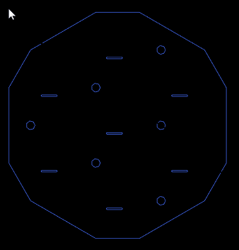
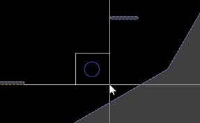
The example (below) shows a 12 sided board with a number of slots and holes (cutouts), this was imported from a DXF file onto the Outline layer. Our aim is to create a PCB board shape in CircuitStudio with the cutouts and keepouts necessary to start laying out and routing the board. The result will be a well defined board with cutouts viewable in 3D.


image


First off we need to define the board outline, this will be created from the outer line segments of the imported drawing. To quickly select just the outer line segments use Home > Select > All followed by Deselect > Inside Area and drag a rectangle as shown below, this must fully enclose all the cutout elements but not fully enclose any line segment (it can partially overlap but not enclose). Alternatively you can click on each of the line segments (holding SHIFT to add to the selection) but some of these can be tricky as the shape is off grid.


image


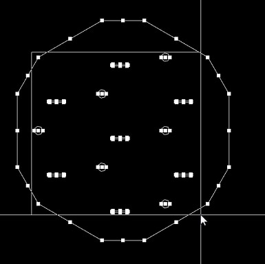
You should end up with just the outer segments selected after using the Deselect command.


image


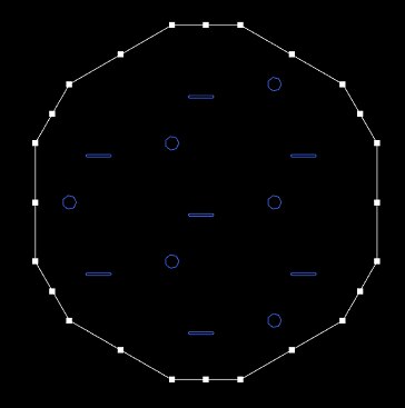
Use Home > Board Shape > Define From Selected Objects to create the board outline shape.


Whilst we have the outline segments still selected let's create a copy to use as the keepout layer which will prevent the router from straying outside the board, we will leave the existing segments on the Outline layer as we may want to use this when generating Gerber files. Follow closely as we are trying to do this with without having to keep re-selecting the outline.


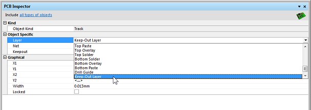
To start creating a copy use Home > Copy then click a suitable point to act as a reference. Change the layer of the existing selected items from Outline to Keep-Out Layer -- enable the Object Inspector (View > Object Inspector) and change the Layer to Keep-Out Layer using the drop down.


image


Use Home > Paste to place the copy we made earlier back onto the Outline layer (the copy was made from the Outline layer and so will paste back to this layer) making sure the copy is aligned with the original.


We now have a keepout boundary that exactly matches the board shape, a drawing of the board outline on the Outline layer and next need to create the cutouts. For each cutout (slots and holes in this example), drag across to select one cutout.


image


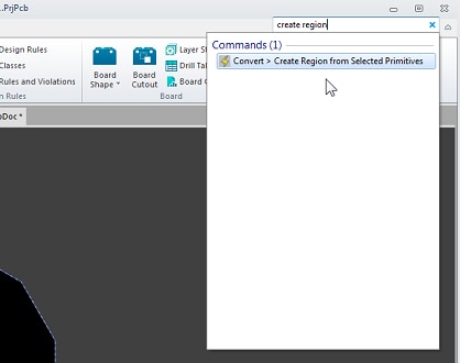
In the search box at the top right type in CREATE REGION and select the Convert > Create Region From Selected Primitives command that is found. We have to use this technique because the command does not have a button or menu option.


image


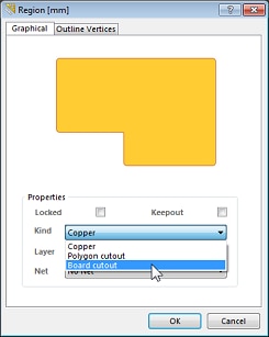
A new region is created but we need to change this to be a cutout so right click on the newly created region, select Properties and change Kind to Board Cutout. Repeat for every cutout and we're done.


image


All done, let's see the results in 3D by selecting View > Switch to 3D. You should have something like below of a complex board shape with many cutouts.


image

  • Sign in to reply
  • baamdesign
    baamdesign over 6 years ago

    Just what I was looking for. Strange that Altium hides the option for the change to region.

    But it works perfectly. Thanks.

    • Cancel
    • Vote Up 0 Vote Down
    • Sign in to reply
    • More
    • Cancel
element14 Community

element14 is the first online community specifically for engineers. Connect with your peers and get expert answers to your questions.

  • Members
  • Learn
  • Technologies
  • Challenges & Projects
  • Products
  • Store
  • About Us
  • Feedback & Support
  • FAQs
  • Terms of Use
  • Privacy Policy
  • Legal and Copyright Notices
  • Sitemap
  • Cookies

An Avnet Company © 2025 Premier Farnell Limited. All Rights Reserved.

Premier Farnell Ltd, registered in England and Wales (no 00876412), registered office: Farnell House, Forge Lane, Leeds LS12 2NE.

ICP 备案号 10220084.

Follow element14

  • X
  • Facebook
  • linkedin
  • YouTube