

We are pleased to announce the new update of CircuitStudio is now available for download. You can install version 1.2.0.37 via the Update System in CircuitStudio.
To install the update:
- Select View > Start to open the Home page
- Select Extensions & Updates link in the Tasks pane
- From the Extensions and Updates page, click the Updates tab
- Click the CircuitStudio 1.2.0 (build 37) update link to start the update process.
Alternatively, the new installer can be downloaded from the CircuitStudio Professional PCB design tool | CircuitStudio page.
I managed to pull together a list of the changes that will be rolled out. Of course you can get this information from the release notes, but here’s one for the folks who don’t like reading too many bullet points from a HTML page 
- F1 Help navigation to documentation pages has been improved – Pretty much self-explanatory.
- My Account Page help links have been updated – There is now a link in the “My Account” page which links to a page in the documentation that shows step-by-step guidance on installing/activating a new standalone license. Pressing F1 key from this page also takes the user to the documentation main page from where all links have been updated.
- Via dragging no longer causes the vias to disconnect from traces when two or more vias are on the same layer and connected to three or more traces. – Self explanatory again!
- Pad objects now support square and slotted holes. – Doesn’t need too much to convey the message.
- Create New Project now uses the Location setting correctly.
- PCB Component Annotation Tool has been added to the Tools ribbon menu.

7. When using an evaluation license you are now informed of how many days are left before expiry
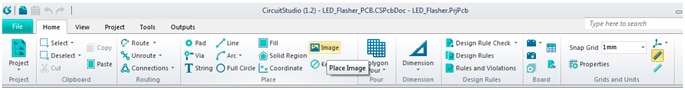
8. Support for placing PCB Images has been added to the Home ribbon menu.
9. STEP output options have been updated.
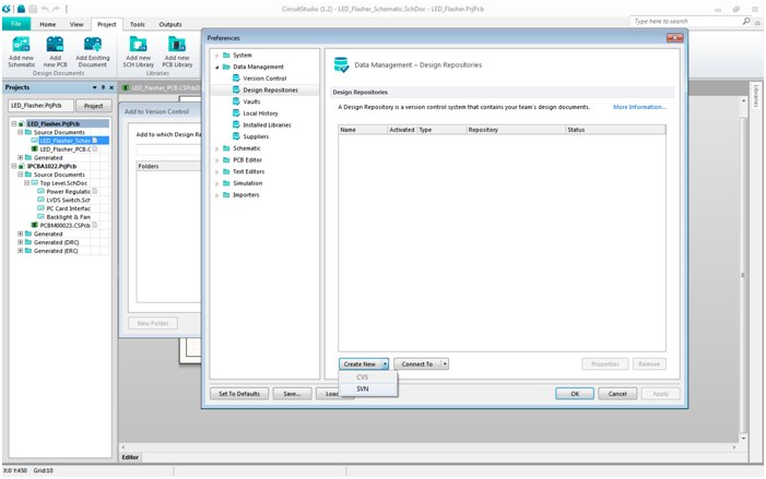
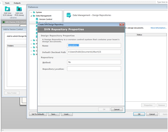
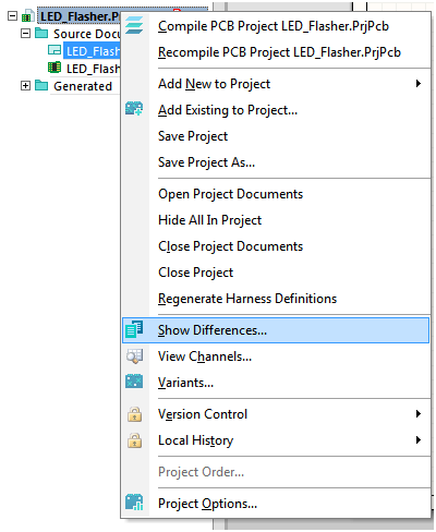
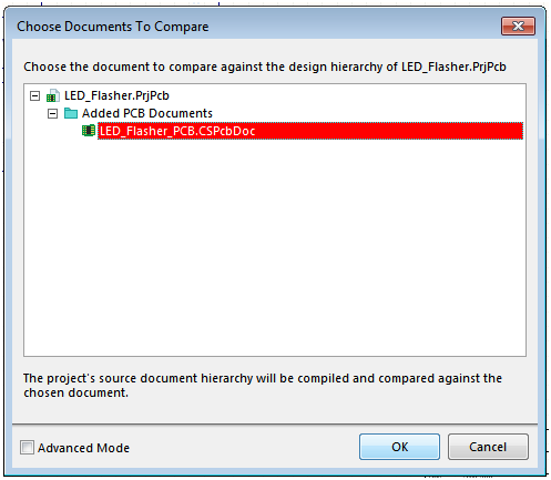
10. Subversion (SVN) support has been added. You can add your document to version control from the right click context menu on the selected document and selecting “Add to Version Control”.
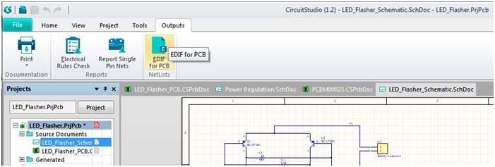
11. The ability to generate an EDIF Netlist has been added. The new command can be found on the Output ribbon of the Schematic editor.

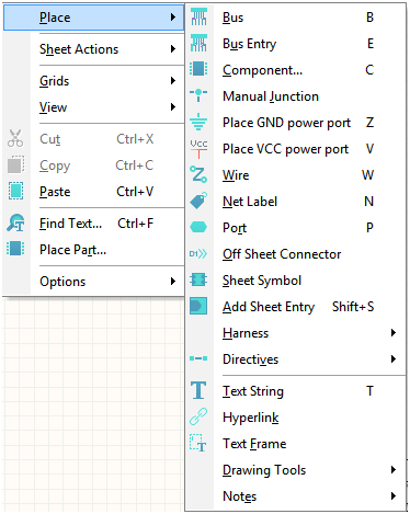
12. Additional Schematic and PCB shortcut keys have been added for common object placement commands. See the Shortcuts panel (Place section) for a complete listing.
13. Visual docking arrows are now shown when moving Panels.
14. The PCB Design Rule report no longer displays unsupported rule types. – This is project specific and would change on a case-by-case basis.
15. Rearranging (dragging and dropping) library documents within the Projects Panel has been improved. – Remember those times when the project panel used to be over crowded with “Free Documents” and you could not get rid of them? Well, that’s been fixed now.