element14 Community
element14 Community
    Register Log In
  • Site
  • Search
  • Log In Register
  • Community Hub
    Community Hub
    • What's New on element14
    • Feedback and Support
    • Benefits of Membership
    • Personal Blogs
    • Members Area
    • Achievement Levels
  • Learn
    Learn
    • Ask an Expert
    • eBooks
    • element14 presents
    • Learning Center
    • Tech Spotlight
    • STEM Academy
    • Webinars, Training and Events
    • Learning Groups
  • Technologies
    Technologies
    • 3D Printing
    • FPGA
    • Industrial Automation
    • Internet of Things
    • Power & Energy
    • Sensors
    • Technology Groups
  • Challenges & Projects
    Challenges & Projects
    • Design Challenges
    • element14 presents Projects
    • Project14
    • Arduino Projects
    • Raspberry Pi Projects
    • Project Groups
  • Products
    Products
    • Arduino
    • Avnet & Tria Boards Community
    • Dev Tools
    • Manufacturers
    • Multicomp Pro
    • Product Groups
    • Raspberry Pi
    • RoadTests & Reviews
  • About Us
  • Store
    Store
    • Visit Your Store
    • Choose another store...
      • Europe
      •  Austria (German)
      •  Belgium (Dutch, French)
      •  Bulgaria (Bulgarian)
      •  Czech Republic (Czech)
      •  Denmark (Danish)
      •  Estonia (Estonian)
      •  Finland (Finnish)
      •  France (French)
      •  Germany (German)
      •  Hungary (Hungarian)
      •  Ireland
      •  Israel
      •  Italy (Italian)
      •  Latvia (Latvian)
      •  
      •  Lithuania (Lithuanian)
      •  Netherlands (Dutch)
      •  Norway (Norwegian)
      •  Poland (Polish)
      •  Portugal (Portuguese)
      •  Romania (Romanian)
      •  Russia (Russian)
      •  Slovakia (Slovak)
      •  Slovenia (Slovenian)
      •  Spain (Spanish)
      •  Sweden (Swedish)
      •  Switzerland(German, French)
      •  Turkey (Turkish)
      •  United Kingdom
      • Asia Pacific
      •  Australia
      •  China
      •  Hong Kong
      •  India
      • Japan
      •  Korea (Korean)
      •  Malaysia
      •  New Zealand
      •  Philippines
      •  Singapore
      •  Taiwan
      •  Thailand (Thai)
      • Vietnam
      • Americas
      •  Brazil (Portuguese)
      •  Canada
      •  Mexico (Spanish)
      •  United States
      Can't find the country/region you're looking for? Visit our export site or find a local distributor.
  • Translate
  • Profile
  • Settings
Altium CircuitStudio
  • Products
  • Manufacturers
  • Altium CircuitStudio
  • More
  • Cancel
Altium CircuitStudio
Altium CircuitStudio Forum PolyGon Pours
  • Blog
  • Forum
  • Documents
  • Events
  • Polls
  • Members
  • Mentions
  • Sub-Groups
  • Tags
  • More
  • Cancel
  • New
Join Altium CircuitStudio to participate - click to join for free!
Actions
  • Share
  • More
  • Cancel
Forum Thread Details
  • Locked Locked
  • Replies 3 replies
  • Subscribers 88 subscribers
  • Views 1008 views
  • Users 0 members are here
Related
This discussion has been locked.
You can no longer post new replies to this discussion. If you have a question you can start a new discussion

PolyGon Pours

batista
batista over 5 years ago

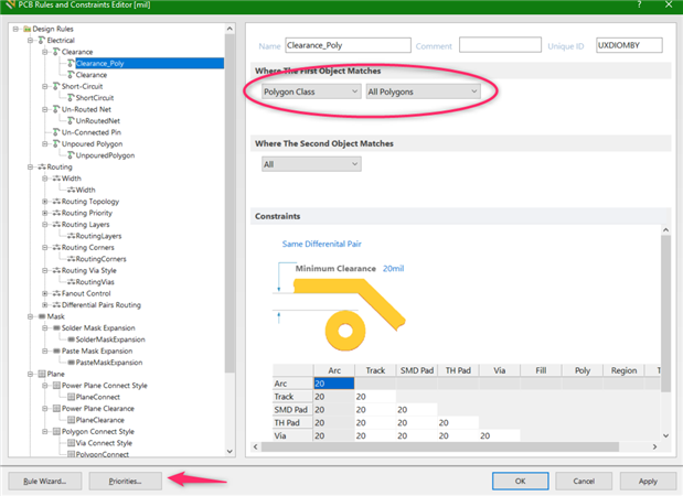
Criei um pequeno projeto no CIRCUITSTUDIO (comprei há pouco tempo aqui mesmo NEWARK ) para testa a ferramenta PolyGon Pour consigo redimensionar até ai tudo bem, mas quando tento mudar o espaço entre PADS e NETS ( Clearance )

o comando não funciona digitei vários valores nesta área ( ARC APPROXIMATION - MAXIMUM DEVIATION FROM PERFECT ) EX: 0.2mm, 0.4 ou 0.6 clik em ok e não muda nada

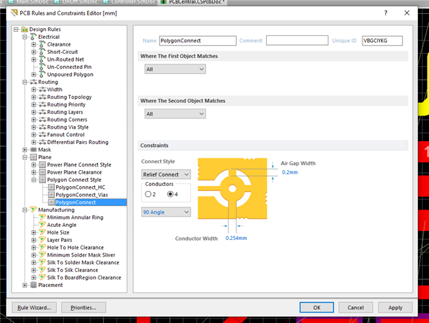
criei uma regra conforme a imagem abaixo também não muda nada. alguém pode me informar o que está acontecendo.


I created a small project in CIRCUITSTUDIO (recently bought here NEWARK) to test the PolyGon Pour tool  I can resize it so far so good, but when I try to change the space between PADS and NETS (Clearance) the command

does not work I entered several values in this area  (ARC APPROXIMATION - MAXIMUM DEVIATION FROM PERFECT) EX: 0.2mm, 0.4 or 0.6 click ok and nothing changes

I created a rule as the image below also does not change anything. can someone tell me what's going on.


imageimage

  • Cancel
  • pizutti
    pizutti over 5 years ago

    The Polygon clearence have a dedicated clearence menu for it, it's on Plane -> Polygon Connect Style


    image

    • Cancel
    • Vote Up 0 Vote Down
    • Cancel
  • tarribred61
    tarribred61 over 5 years ago in reply to pizutti

    Hi,

    I think the polygon connect style rule is only for control of the connection of pins to the polygon.


    To adjust the clearance of the polygon to other nets, polygons and such, you would use the clearance rules.  If you want a polygon to have its own special clearance then make a rule specific to the polygon by using the polygon classes.  Also, I suspect the issue with the problem is due to rule priority setting.


    Here is my rule that works for a simple design that has one polygon flood on the bottom layer.  I named it Clearance_Poly and set first object to Polygon Class and All Polygons.  Then set the clearance you want.  Also, set this to have priority over the default clearance.


    If you have other polygons with different needs you need to define polygon classes and add the polygons to the classes. This might be something like a class for polygons on the bottom layer or some that are specific to high voltage nets, for example.

    image

    • Cancel
    • Vote Up 0 Vote Down
    • Cancel
  • tarribred61
    tarribred61 over 5 years ago in reply to tarribred61

    Also, since you are investigating use of CS and polygons you may want to know that; if you put a number of Polygon pours you may find you want to control the order of polygon pours.  CircuitStudio is a bit weak in this as compared to Altium Designer which has a pour manager tool.


    CircuitStudio, does not have a pour manager tool and so you can work around this by sending polygons forward or back. Basically, pick the polygon and right click to get the context menus. Choose Polygon Actions and then either "Bring to front" or "Send to back".  This will control pour order on the layer.  I don't know of anyway to actual view and confirm the pour order though.  So, if you had a PCB with a lot of complex overlapping polygon pours you would need to be careful or pay for a more featured Altium Designer seat.


    image

    • Cancel
    • Vote Up 0 Vote Down
    • Cancel
element14 Community

element14 is the first online community specifically for engineers. Connect with your peers and get expert answers to your questions.

  • Members
  • Learn
  • Technologies
  • Challenges & Projects
  • Products
  • Store
  • About Us
  • Feedback & Support
  • FAQs
  • Terms of Use
  • Privacy Policy
  • Legal and Copyright Notices
  • Sitemap
  • Cookies

An Avnet Company © 2026 Premier Farnell Limited. All Rights Reserved.

Premier Farnell Ltd, registered in England and Wales (no 00876412), registered office: Farnell House, Forge Lane, Leeds LS12 2NE.

ICP 备案号 10220084.

Follow element14

  • X
  • Facebook
  • linkedin
  • YouTube