element14 Community
element14 Community
    Register Log In
  • Site
  • Search
  • Log In Register
  • Community Hub
    Community Hub
    • What's New on element14
    • Feedback and Support
    • Benefits of Membership
    • Personal Blogs
    • Members Area
    • Achievement Levels
  • Learn
    Learn
    • Ask an Expert
    • eBooks
    • element14 presents
    • Learning Center
    • Tech Spotlight
    • STEM Academy
    • Webinars, Training and Events
    • Learning Groups
  • Technologies
    Technologies
    • 3D Printing
    • FPGA
    • Industrial Automation
    • Internet of Things
    • Power & Energy
    • Sensors
    • Technology Groups
  • Challenges & Projects
    Challenges & Projects
    • Design Challenges
    • element14 presents Projects
    • Project14
    • Arduino Projects
    • Raspberry Pi Projects
    • Project Groups
  • Products
    Products
    • Arduino
    • Avnet & Tria Boards Community
    • Dev Tools
    • Manufacturers
    • Multicomp Pro
    • Product Groups
    • Raspberry Pi
    • RoadTests & Reviews
  • About Us
  • Store
    Store
    • Visit Your Store
    • Choose another store...
      • Europe
      •  Austria (German)
      •  Belgium (Dutch, French)
      •  Bulgaria (Bulgarian)
      •  Czech Republic (Czech)
      •  Denmark (Danish)
      •  Estonia (Estonian)
      •  Finland (Finnish)
      •  France (French)
      •  Germany (German)
      •  Hungary (Hungarian)
      •  Ireland
      •  Israel
      •  Italy (Italian)
      •  Latvia (Latvian)
      •  
      •  Lithuania (Lithuanian)
      •  Netherlands (Dutch)
      •  Norway (Norwegian)
      •  Poland (Polish)
      •  Portugal (Portuguese)
      •  Romania (Romanian)
      •  Russia (Russian)
      •  Slovakia (Slovak)
      •  Slovenia (Slovenian)
      •  Spain (Spanish)
      •  Sweden (Swedish)
      •  Switzerland(German, French)
      •  Turkey (Turkish)
      •  United Kingdom
      • Asia Pacific
      •  Australia
      •  China
      •  Hong Kong
      •  India
      • Japan
      •  Korea (Korean)
      •  Malaysia
      •  New Zealand
      •  Philippines
      •  Singapore
      •  Taiwan
      •  Thailand (Thai)
      • Vietnam
      • Americas
      •  Brazil (Portuguese)
      •  Canada
      •  Mexico (Spanish)
      •  United States
      Can't find the country/region you're looking for? Visit our export site or find a local distributor.
  • Translate
  • Profile
  • Settings
Altium CircuitStudio
  • Products
  • Manufacturers
  • Altium CircuitStudio
  • More
  • Cancel
Altium CircuitStudio
Altium CircuitStudio Forum DRC Rule minimum copper width
  • Blog
  • Forum
  • Documents
  • Events
  • Polls
  • Members
  • Mentions
  • Sub-Groups
  • Tags
  • More
  • Cancel
  • New
Join Altium CircuitStudio to participate - click to join for free!
Actions
  • Share
  • More
  • Cancel
Forum Thread Details
  • Locked Locked
  • Replies 5 replies
  • Subscribers 88 subscribers
  • Views 1951 views
  • Users 0 members are here
Related
This discussion has been locked.
You can no longer post new replies to this discussion. If you have a question you can start a new discussion

DRC Rule minimum copper width

mf_ibfeew
mf_ibfeew over 4 years ago

Hello,

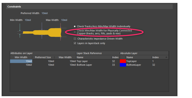
In the design rules I can define rules for minimum trace width. this works well for standard traces.

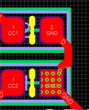
But the appended picture shows a problem with a minimum copper width in a special case. The net connects to the pad only with a very small edge, but none of the design-rules catches this event. Neither  the "unrouted" nor the "minimum trackwidth" - rules are complaining at this picture. Is there a rule which marks this picture as failure? How can I avoid such a situation? (the production of this board could easily produce an error at this point, it was pure luck that I catched this glitch)

Nice weekend, Maik Freitag

Attachments:
image
  • Cancel
  • tarribred61
    tarribred61 over 4 years ago

    Hi,


    The rules are similar to the Altium Designer rules for width.  I found them for AD18 as described here: https://www.altium.com/documentation/altium-designer/pcb-dlg-maxminwidthrule-framewidth-ad?version=18.1


    Did you try the selection for physical connected copper?  I'm not sure but otherwise I think it only checks the routing meets the expected rules and would not catch what you noted.

    image


    Darn, you got me curious and now I'm going to have to try this myself.

    • Cancel
    • Vote Up 0 Vote Down
    • Cancel
  • tarribred61
    tarribred61 over 4 years ago in reply to tarribred61

    I confirmed that for CS1.5.2 using the width rule with the check box set for physically connected copper that it caught the condition I artificially made for a small connection area. It did this using both batch and on-line DRC.

    Screen shot below shows what I see for detecting a copper connection less than the rule of 10mil.

    image

    • Cancel
    • Vote Up 0 Vote Down
    • Cancel
  • mf_ibfeew
    mf_ibfeew over 4 years ago in reply to tarribred61

    Thanks for your effort.

    At  first I have to admit that until now I have overlooked and ignored the 4 checkboxes to the right of the min/max-sketch.

    The "check for physically connected copper" improves the situation and detects at least problems if 2 wires don't overlap properly. (middle of my picture, top half).

    The insufficient connection from wire to pad (bottom of the picture) is still not flagged as an error.

    I have now tried to play with another design (to exclude project-specific failures), but same behavior.image

    rule settings (now with the found physical-copper-switch set):

    image

    Can you upload a picture from your small-connect-test?

    Maik

    • Cancel
    • Vote Up 0 Vote Down
    • Cancel
  • mf_ibfeew
    mf_ibfeew over 4 years ago in reply to tarribred61

    thanks for the picture. It has clarified something and after some "play around" I think there are some bugs in the width-calculation for "special cases".

    If I connect the wire like your example (wire straight to the pad) I get an error (like you). (pic1)

    If my wire touches the corner of the pad (45degree wire), I get no error. (pic2)

    If I have a combination of 1+2 (straight wire connection and a 45 degree touch-connection), I also get no error. Also not on the place where pic1 showed an error.

    This situation is not ideal for pcb-check before manufacturing. Hopefully this will be fixed in the soon-to-be-released circuitmaker pro (probably around 2025...2027?).

    So for now I have to accept this restriction.

    image

    image

    image

    • Cancel
    • Vote Up 0 Vote Down
    • Cancel
  • tarribred61
    tarribred61 over 4 years ago in reply to mf_ibfeew

    I rechecked my example and found that there is a point of contact where the unrouted net length goes to 0 but the DRC does not indicate the rule violation.  If I move the net a little bit to give more contact then the rule shows the violation. 


    It is possible that Altium Designer also does this.  I have posted this issue in the CircuitMaker Pro beta forum since it seems to have the same issue.

    • Cancel
    • Vote Up 0 Vote Down
    • Cancel
element14 Community

element14 is the first online community specifically for engineers. Connect with your peers and get expert answers to your questions.

  • Members
  • Learn
  • Technologies
  • Challenges & Projects
  • Products
  • Store
  • About Us
  • Feedback & Support
  • FAQs
  • Terms of Use
  • Privacy Policy
  • Legal and Copyright Notices
  • Sitemap
  • Cookies

An Avnet Company © 2025 Premier Farnell Limited. All Rights Reserved.

Premier Farnell Ltd, registered in England and Wales (no 00876412), registered office: Farnell House, Forge Lane, Leeds LS12 2NE.

ICP 备案号 10220084.

Follow element14

  • X
  • Facebook
  • linkedin
  • YouTube