element14 Community
element14 Community
    Register Log In
  • Site
  • Search
  • Log In Register
  • Community Hub
    Community Hub
    • What's New on element14
    • Feedback and Support
    • Benefits of Membership
    • Personal Blogs
    • Members Area
    • Achievement Levels
  • Learn
    Learn
    • Ask an Expert
    • eBooks
    • element14 presents
    • Learning Center
    • Tech Spotlight
    • STEM Academy
    • Webinars, Training and Events
    • Learning Groups
  • Technologies
    Technologies
    • 3D Printing
    • FPGA
    • Industrial Automation
    • Internet of Things
    • Power & Energy
    • Sensors
    • Technology Groups
  • Challenges & Projects
    Challenges & Projects
    • Design Challenges
    • element14 presents Projects
    • Project14
    • Arduino Projects
    • Raspberry Pi Projects
    • Project Groups
  • Products
    Products
    • Arduino
    • Avnet Boards Community
    • Dev Tools
    • Manufacturers
    • Multicomp Pro
    • Product Groups
    • Raspberry Pi
    • RoadTests & Reviews
  • About Us
  • Store
    Store
    • Visit Your Store
    • Choose another store...
      • Europe
      •  Austria (German)
      •  Belgium (Dutch, French)
      •  Bulgaria (Bulgarian)
      •  Czech Republic (Czech)
      •  Denmark (Danish)
      •  Estonia (Estonian)
      •  Finland (Finnish)
      •  France (French)
      •  Germany (German)
      •  Hungary (Hungarian)
      •  Ireland
      •  Israel
      •  Italy (Italian)
      •  Latvia (Latvian)
      •  
      •  Lithuania (Lithuanian)
      •  Netherlands (Dutch)
      •  Norway (Norwegian)
      •  Poland (Polish)
      •  Portugal (Portuguese)
      •  Romania (Romanian)
      •  Russia (Russian)
      •  Slovakia (Slovak)
      •  Slovenia (Slovenian)
      •  Spain (Spanish)
      •  Sweden (Swedish)
      •  Switzerland(German, French)
      •  Turkey (Turkish)
      •  United Kingdom
      • Asia Pacific
      •  Australia
      •  China
      •  Hong Kong
      •  India
      •  Korea (Korean)
      •  Malaysia
      •  New Zealand
      •  Philippines
      •  Singapore
      •  Taiwan
      •  Thailand (Thai)
      • Americas
      •  Brazil (Portuguese)
      •  Canada
      •  Mexico (Spanish)
      •  United States
      Can't find the country/region you're looking for? Visit our export site or find a local distributor.
  • Translate
  • Profile
  • Settings
Altium CircuitStudio
  • Products
  • Manufacturers
  • Altium CircuitStudio
  • More
  • Cancel
Altium CircuitStudio
Altium CircuitStudio Forum Via to pad clearance design rule
  • Blog
  • Forum
  • Documents
  • Events
  • Polls
  • Members
  • Mentions
  • Sub-Groups
  • Tags
  • More
  • Cancel
  • New
Join Altium CircuitStudio to participate - click to join for free!
Actions
  • Share
  • More
  • Cancel
Forum Thread Details
  • State Verified Answer
  • Locked Locked
  • Replies 6 replies
  • Subscribers 92 subscribers
  • Views 5016 views
  • Users 0 members are here
Related
This discussion has been locked.
You can no longer post new replies to this discussion. If you have a question you can start a new discussion

Via to pad clearance design rule

jallard
jallard over 8 years ago

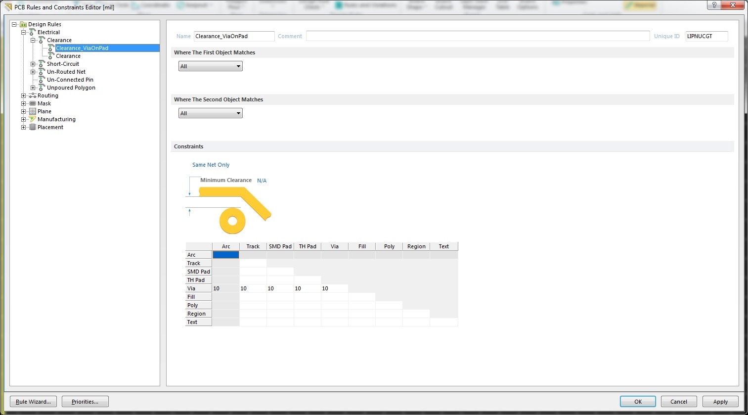
Placing a via over the top of a SMT pad with the same net does not create a design rule error. Is there a way to add a rule prohibiting this?


I tried creating a clearance rule for "same net only" with all the clearance matrix values set to zero except Via-to-SMD Pad and Via-to-TH Pad. Unfortunately, this generates a Via-to-track clearance violation on all vias. I'm assuming zero is not sufficient to disable the matrix connection (e.g., setting Via-to-Track == 0, doesn't disable this clearance check).


Seems like there should be a way to prevent vias over the top of SMD pads. Am I missing something?

  • Cancel

Top Replies

  • adamwebber
    adamwebber over 8 years ago +2 verified
    So I've never had an issue with this but suddenly I am questioning all of my previous work. I have used Altium extensively and it is so easy to create simple rules to avoid placing vias on pads. CircuitStudio…
  • jallard
    jallard over 8 years ago in reply to adamwebber +1
    Wonderful! Thank you. -1 in the Minimum clearance. Seems like something that should be documented. :-) This works great, which leads to another issue. Some pads and fills require vias in the middle of…
  • songshome
    songshome over 8 years ago in reply to jallard +1
    Firstly, thank you James Clark for -1. To Jim, you can try this: make rule for netclass, then export it and change netclass to padclass with text editor and then import rule. I did not try it, but it should…
Parents
  • adamwebber
    0 adamwebber over 8 years ago

    So I've never had an issue with this but suddenly I am questioning all of my previous work.  I have used Altium extensively and it is so easy to create simple rules to avoid placing vias on pads.  CircuitStudio is not quite as simple.  You can still use all of the functionality from Altium by exporting the rules and then writing them as a text file then importing them back in.  Sometimes it's necessary but it sucks. 


    I did try this and I was able to successfully create a via on pad rule by using the built-in PCB Rules and Constraints Editor.  Right-Click on your screen and select "Design" and then "Rules" and perform the following steps:

    1-Duplicate your clearance rules.

    2-Rename it to something smug.

    3-Change the priority so that it is higher than standard clearance.

    4-Select your first and second object matching if you wish.  I kept them both as "All".

    5-Select "Same Net Only" as your constraints.

    6-Select the Minimum Clearance and change it to -1.  THIS IS YOUR VITAL STEP.  You cannot change each individual clearance to -1.  You must do it as a whole.

    7-Change your clearance for Vias to whatever spacing you want.

    8-Press OK.

    image

    • Cancel
    • Vote Up +2 Vote Down
    • Cancel
  • jallard
    0 jallard over 8 years ago in reply to adamwebber

    Wonderful! Thank you.


    -1 in the Minimum clearance. Seems like something that should be documented. :-)


    This works great, which leads to another issue. Some pads and fills require vias in the middle of the pad, e.g., thermal pads on the bottom of IC's. It would be nice to exclude these from the clearance rule but I don't see a way, since object matching only works for net classes and layers, not pad classes. Unless there's a trick? Maybe -2 in some box somewhere? :-)

    • Cancel
    • Vote Up +1 Vote Down
    • Cancel
  • songshome
    0 songshome over 8 years ago in reply to jallard

    Firstly, thank you James Clark for -1.

    To Jim, you can try this: make rule for netclass, then export it and change netclass to padclass with text editor and then import rule. I did not try it, but it should work. I hope, Altium can add pad and padclass to clearance rules.

    • Cancel
    • Vote Up +1 Vote Down
    • Cancel
  • jallard
    0 jallard over 8 years ago in reply to songshome

    This works if I create a padclass that includes all the pads EXCEPT the pads that I don't want a via-to-pad clearance rule on. This is okay, but it would be nicer to somehow create a rule the excludes certain pads instead of having to include all the pads. Otherwise, I have to remember to update the padclass when new pads are added.


    My procedure is:

    1) Create a Pad class containing all the pads except the pads that I want to allow vias in. (name it "viacheck" or something like this).

    2) Create a clearance rule with "SameNetOnly" and -1 global clearance.

    3) Enter a clearance value in the via-to-SMD pad matrix cell.

    4) Export the rules.

    5) Edit the SCOPE2EXPRESSION value to be "InPadClass('viacheck')". Leave SCOPE1EXPRESSION set to "All".

    6) Import the edited rules.


    This seems to work.

    • Cancel
    • Vote Up 0 Vote Down
    • Cancel
Reply
  • jallard
    0 jallard over 8 years ago in reply to songshome

    This works if I create a padclass that includes all the pads EXCEPT the pads that I don't want a via-to-pad clearance rule on. This is okay, but it would be nicer to somehow create a rule the excludes certain pads instead of having to include all the pads. Otherwise, I have to remember to update the padclass when new pads are added.


    My procedure is:

    1) Create a Pad class containing all the pads except the pads that I want to allow vias in. (name it "viacheck" or something like this).

    2) Create a clearance rule with "SameNetOnly" and -1 global clearance.

    3) Enter a clearance value in the via-to-SMD pad matrix cell.

    4) Export the rules.

    5) Edit the SCOPE2EXPRESSION value to be "InPadClass('viacheck')". Leave SCOPE1EXPRESSION set to "All".

    6) Import the edited rules.


    This seems to work.

    • Cancel
    • Vote Up 0 Vote Down
    • Cancel
Children
No Data
element14 Community

element14 is the first online community specifically for engineers. Connect with your peers and get expert answers to your questions.

  • Members
  • Learn
  • Technologies
  • Challenges & Projects
  • Products
  • Store
  • About Us
  • Feedback & Support
  • FAQs
  • Terms of Use
  • Privacy Policy
  • Legal and Copyright Notices
  • Sitemap
  • Cookies

An Avnet Company © 2025 Premier Farnell Limited. All Rights Reserved.

Premier Farnell Ltd, registered in England and Wales (no 00876412), registered office: Farnell House, Forge Lane, Leeds LS12 2NE.

ICP 备案号 10220084.

Follow element14

  • X
  • Facebook
  • linkedin
  • YouTube