element14 Community
element14 Community
    Register Log In
  • Site
  • Search
  • Log In Register
  • Community Hub
    Community Hub
    • What's New on element14
    • Feedback and Support
    • Benefits of Membership
    • Personal Blogs
    • Members Area
    • Achievement Levels
  • Learn
    Learn
    • Ask an Expert
    • eBooks
    • element14 presents
    • Learning Center
    • Tech Spotlight
    • STEM Academy
    • Webinars, Training and Events
    • Learning Groups
  • Technologies
    Technologies
    • 3D Printing
    • FPGA
    • Industrial Automation
    • Internet of Things
    • Power & Energy
    • Sensors
    • Technology Groups
  • Challenges & Projects
    Challenges & Projects
    • Design Challenges
    • element14 presents Projects
    • Project14
    • Arduino Projects
    • Raspberry Pi Projects
    • Project Groups
  • Products
    Products
    • Arduino
    • Avnet & Tria Boards Community
    • Dev Tools
    • Manufacturers
    • Multicomp Pro
    • Product Groups
    • Raspberry Pi
    • RoadTests & Reviews
  • About Us
  • Store
    Store
    • Visit Your Store
    • Choose another store...
      • Europe
      •  Austria (German)
      •  Belgium (Dutch, French)
      •  Bulgaria (Bulgarian)
      •  Czech Republic (Czech)
      •  Denmark (Danish)
      •  Estonia (Estonian)
      •  Finland (Finnish)
      •  France (French)
      •  Germany (German)
      •  Hungary (Hungarian)
      •  Ireland
      •  Israel
      •  Italy (Italian)
      •  Latvia (Latvian)
      •  
      •  Lithuania (Lithuanian)
      •  Netherlands (Dutch)
      •  Norway (Norwegian)
      •  Poland (Polish)
      •  Portugal (Portuguese)
      •  Romania (Romanian)
      •  Russia (Russian)
      •  Slovakia (Slovak)
      •  Slovenia (Slovenian)
      •  Spain (Spanish)
      •  Sweden (Swedish)
      •  Switzerland(German, French)
      •  Turkey (Turkish)
      •  United Kingdom
      • Asia Pacific
      •  Australia
      •  China
      •  Hong Kong
      •  India
      • Japan
      •  Korea (Korean)
      •  Malaysia
      •  New Zealand
      •  Philippines
      •  Singapore
      •  Taiwan
      •  Thailand (Thai)
      • Vietnam
      • Americas
      •  Brazil (Portuguese)
      •  Canada
      •  Mexico (Spanish)
      •  United States
      Can't find the country/region you're looking for? Visit our export site or find a local distributor.
  • Translate
  • Profile
  • Settings
Altium CircuitStudio
  • Products
  • Manufacturers
  • Altium CircuitStudio
  • More
  • Cancel
Altium CircuitStudio
Altium CircuitStudio Forum Complex shapes for pads
  • Blog
  • Forum
  • Documents
  • Events
  • Polls
  • Members
  • Mentions
  • Sub-Groups
  • Tags
  • More
  • Cancel
  • New
Join Altium CircuitStudio to participate - click to join for free!
Actions
  • Share
  • More
  • Cancel
Forum Thread Details
  • State Verified Answer
  • Locked Locked
  • Replies 8 replies
  • Subscribers 91 subscribers
  • Views 1496 views
  • Users 0 members are here
  • pad
  • library
Related
This discussion has been locked.
You can no longer post new replies to this discussion. If you have a question you can start a new discussion

Complex shapes for pads

frog
frog over 8 years ago

Hi All,

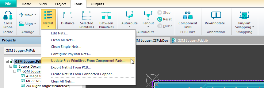
When creating a component footprint I sometimes want something more complex than the standard options (circle, octagon, rectangle, rounded rectangle).  I've found experimentally that I can add multiple pads with the same identifier e.g. for the middle pin and heatsink tab of a SOT-223 and CS recognises that they are both on the same net.  But if I add extra copper (such as an arc) to the footprint then the net isn't assigned automatically and I have to edit the part in the PCB to fix this.  Is there a 'proper' way to attach arbitrary copper to a pad in a library part?


Thanks,

Frog

  • Cancel
  • adamwebber
    0 adamwebber over 8 years ago

    I also have this problem.  As a workaround I have to layout the footprint in the PCB editor instead of the footprint editor.  I'm not entirely fond of doing it this way.

    • Cancel
    • Vote Up 0 Vote Down
    • Cancel
  • alexsander_altium
    0 alexsander_altium over 8 years ago

    I may be misunderstanding but if you want to create custom pad shapes for your component footprints you would have to do this in the PCB library editor. Using the fill feature under the home tab and then double clicking on it afterwards you should be able to assign a net to that copper.

    • Cancel
    • Vote Up 0 Vote Down
    • Cancel
  • frog
    0 frog over 8 years ago in reply to alexsander_altium

    That's more or less what I'm doing at the moment, but the problem is that the net name is likely to be different each time the part is used in a PCB.  Pads automatically update the net name from corresponding pin in the netlist, but fills etc don't do this and so additional manual steps are needed.  So my question is, is there a way, within the PCB library editor, to tell a copper feature that it should take the net name of a particular pin in the netlist (or the same net name as a given pad).

    • Cancel
    • Vote Up 0 Vote Down
    • Cancel
  • alexsander_altium
    0 alexsander_altium over 8 years ago in reply to frog

    I see what you're saying. I'm not sure, i'll ask. jamesharrimanaltium would you know?

    • Cancel
    • Vote Up 0 Vote Down
    • Cancel
  • alexsander_altium
    0 alexsander_altium over 8 years ago in reply to frog

    are you working on version 1.4.1?


    get the netlist clean and see if it continues, run the command update free primitives from component pads.

    image


    clear error markers and rerun DRC and see if it is clear for those parts, it should be Then, let us know if the issue comes back, and to try and record the sequence of events that leads to the disconnect. There MUST be a pad somewhere inside the construct that can receive a net, which can then be passed to the connected primitives If it is just copper, with no pad to receive a net, it wont work.

    • Cancel
    • Vote Up 0 Vote Down
    • Cancel
  • frog
    0 frog over 8 years ago in reply to alexsander_altium

    I wondered what that option was for :-)

    I'll give it a try, thanks.

    • Cancel
    • Vote Up 0 Vote Down
    • Cancel
  • frog
    0 frog over 8 years ago in reply to frog

    It appears that version 1.4.1 *does* pick up the correct netlist for fills that are attached to a pad, but if I set the netlist for a fill back to 'no net' then the above does correctly reassign it to the net of an attached pad.


    Thank you.

    • Cancel
    • Vote Up 0 Vote Down
    • Cancel
  • jamesharrimanaltium
    0 jamesharrimanaltium over 8 years ago in reply to alexsander_altium

    Hi Alexsander,


    I agree update free primitives from component pads is the way to achieve this, rather than within the library editor.

    Best regards,

    James Harriman

    • Cancel
    • Vote Up 0 Vote Down
    • Cancel
element14 Community

element14 is the first online community specifically for engineers. Connect with your peers and get expert answers to your questions.

  • Members
  • Learn
  • Technologies
  • Challenges & Projects
  • Products
  • Store
  • About Us
  • Feedback & Support
  • FAQs
  • Terms of Use
  • Privacy Policy
  • Legal and Copyright Notices
  • Sitemap
  • Cookies

An Avnet Company © 2026 Premier Farnell Limited. All Rights Reserved.

Premier Farnell Ltd, registered in England and Wales (no 00876412), registered office: Farnell House, Forge Lane, Leeds LS12 2NE.

ICP 备案号 10220084.

Follow element14

  • X
  • Facebook
  • linkedin
  • YouTube