element14 Community
element14 Community
    Register Log In
  • Site
  • Search
  • Log In Register
  • About Us
  • Community Hub
    Community Hub
    • What's New on element14
    • Feedback and Support
    • Benefits of Membership
    • Personal Blogs
    • Members Area
    • Achievement Levels
  • Learn
    Learn
    • Ask an Expert
    • eBooks
    • element14 presents
    • Learning Center
    • Tech Spotlight
    • STEM Academy
    • Webinars, Training and Events
    • Learning Groups
  • Technologies
    Technologies
    • 3D Printing
    • FPGA
    • Industrial Automation
    • Internet of Things
    • Power & Energy
    • Sensors
    • Technology Groups
  • Challenges & Projects
    Challenges & Projects
    • Design Challenges
    • element14 presents Projects
    • Project14
    • Arduino Projects
    • Raspberry Pi Projects
    • Project Groups
  • Products
    Products
    • Arduino
    • Avnet Boards Community
    • Dev Tools
    • Manufacturers
    • Multicomp Pro
    • Product Groups
    • Raspberry Pi
    • RoadTests & Reviews
  • Store
    Store
    • Visit Your Store
    • Choose another store...
      • Europe
      •  Austria (German)
      •  Belgium (Dutch, French)
      •  Bulgaria (Bulgarian)
      •  Czech Republic (Czech)
      •  Denmark (Danish)
      •  Estonia (Estonian)
      •  Finland (Finnish)
      •  France (French)
      •  Germany (German)
      •  Hungary (Hungarian)
      •  Ireland
      •  Israel
      •  Italy (Italian)
      •  Latvia (Latvian)
      •  
      •  Lithuania (Lithuanian)
      •  Netherlands (Dutch)
      •  Norway (Norwegian)
      •  Poland (Polish)
      •  Portugal (Portuguese)
      •  Romania (Romanian)
      •  Russia (Russian)
      •  Slovakia (Slovak)
      •  Slovenia (Slovenian)
      •  Spain (Spanish)
      •  Sweden (Swedish)
      •  Switzerland(German, French)
      •  Turkey (Turkish)
      •  United Kingdom
      • Asia Pacific
      •  Australia
      •  China
      •  Hong Kong
      •  India
      •  Korea (Korean)
      •  Malaysia
      •  New Zealand
      •  Philippines
      •  Singapore
      •  Taiwan
      •  Thailand (Thai)
      • Americas
      •  Brazil (Portuguese)
      •  Canada
      •  Mexico (Spanish)
      •  United States
      Can't find the country/region you're looking for? Visit our export site or find a local distributor.
  • Translate
  • Profile
  • Settings
Altium CircuitStudio
  • Products
  • Manufacturers
  • Altium CircuitStudio
  • More
  • Cancel
Altium CircuitStudio
Altium CircuitStudio Forum PCB Footprint pattern generator
  • Blog
  • Forum
  • Documents
  • Events
  • Polls
  • Members
  • Mentions
  • Sub-Groups
  • Tags
  • More
  • Cancel
  • New
Join Altium CircuitStudio to participate - click to join for free!
Actions
  • Share
  • More
  • Cancel
Forum Thread Details
  • State Suggested Answer
  • Locked Locked
  • Replies 3 replies
  • Answers 1 answer
  • Subscribers 88 subscribers
  • Views 1389 views
  • Users 0 members are here
Related
This discussion has been locked.
You can no longer post new replies to this discussion. If you have a question you can start a new discussion

PCB Footprint pattern generator

mtripoli3
mtripoli3 over 7 years ago

Hello,


I started using CS 1.4 about a week ago at the behest of a potentially new client. To get it out of the way, I have been designing PCB's for 40 years (man, I shouldn't be able to say that; I started out on film with tape) and have used OrCAD almost exclusively, Mentor along the way, and now Diptrace almost exclusively (not super great, but does everything I need). I design high-volume consumer electronics for a living. I immediately liked CS from the start, it "feels" very "smooth", the functionality is there, however... I ran into two issues, one of which I raise here.


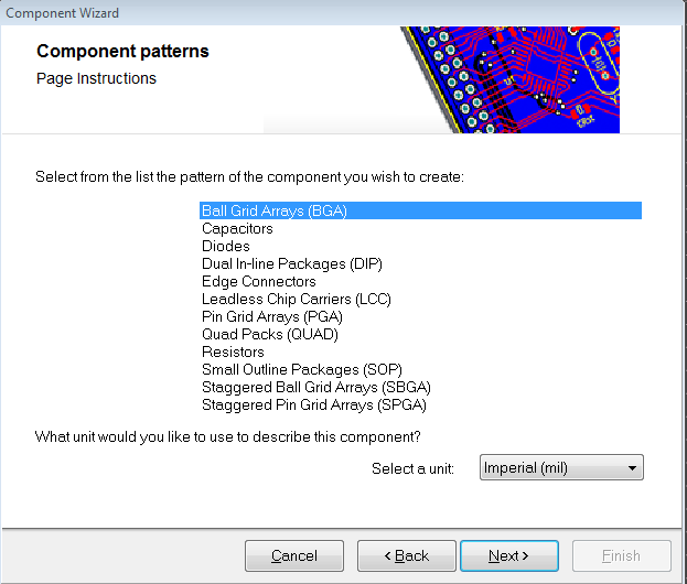
From the start, I needed a new part that will not be found in any library (that I found), specifically, an FV-1 from Spin Semi. Nothing exciting, a 28 pin, 300mil SOIC. Being that I wanted to "fully experience CS" I made the schematic symbol and footprint myself, as opposed to pulling in a 28 pin device and "Saving As". As I made the symbols and footprints, I could not find anywhere any kind of "Pattern Generator" i.e. any kind of "spreadsheet" where you fill in the blanks and it generates the footprint precisely based on the input criteria. Am I overlooking something? Is this "in there" and I haven't found it? I've searched and watched every video on Youtube, nothing. Having to place each pad separately, in any CAD package in 2018, is not expected, but also if not there, makes the "tool" a time-sink instead of profit center. In this case, it was simple part, however, if I had to do something more complicated, I simply couldn't use this software.


So, please let me know, am I overlooking where the "pattern generators" are, or are they simply not there. I'm running the trial, with the expectation to purchase at the end of the trial, however, if both the schematic symbol and PCB footprint requires one to place each pin individually, I'm going to give up on CS right now and continue to use Diptrace. Please do not suggest "just grab a library part and modify it"; that is not an answer. I do this professionally, and need access to all tools that make up a useful CAD tool, not just "copy what others have done".


Thank you,

Mike Tripoli

  • Cancel
Parents
  • e14softwareuk
    0 e14softwareuk over 7 years ago

    Hi Mike, there is a basic footprint wizard available. Open your PCB library and then select Tools | Component Wizard.

    image

    • Cancel
    • Vote Up 0 Vote Down
    • Cancel
Reply
  • e14softwareuk
    0 e14softwareuk over 7 years ago

    Hi Mike, there is a basic footprint wizard available. Open your PCB library and then select Tools | Component Wizard.

    image

    • Cancel
    • Vote Up 0 Vote Down
    • Cancel
Children
No Data
element14 Community

element14 is the first online community specifically for engineers. Connect with your peers and get expert answers to your questions.

  • Members
  • Learn
  • Technologies
  • Challenges & Projects
  • Products
  • Store
  • About Us
  • Feedback & Support
  • FAQs
  • Terms of Use
  • Privacy Policy
  • Legal and Copyright Notices
  • Sitemap
  • Cookies

An Avnet Company © 2025 Premier Farnell Limited. All Rights Reserved.

Premier Farnell Ltd, registered in England and Wales (no 00876412), registered office: Farnell House, Forge Lane, Leeds LS12 2NE.

ICP 备案号 10220084.

Follow element14

  • X
  • Facebook
  • linkedin
  • YouTube