element14 Community
element14 Community
    Register Log In
  • Site
  • Search
  • Log In Register
  • Community Hub
    Community Hub
    • What's New on element14
    • Feedback and Support
    • Benefits of Membership
    • Personal Blogs
    • Members Area
    • Achievement Levels
  • Learn
    Learn
    • Ask an Expert
    • eBooks
    • element14 presents
    • Learning Center
    • Tech Spotlight
    • STEM Academy
    • Webinars, Training and Events
    • Learning Groups
  • Technologies
    Technologies
    • 3D Printing
    • FPGA
    • Industrial Automation
    • Internet of Things
    • Power & Energy
    • Sensors
    • Technology Groups
  • Challenges & Projects
    Challenges & Projects
    • Design Challenges
    • element14 presents Projects
    • Project14
    • Arduino Projects
    • Raspberry Pi Projects
    • Project Groups
  • Products
    Products
    • Arduino
    • Avnet & Tria Boards Community
    • Dev Tools
    • Manufacturers
    • Multicomp Pro
    • Product Groups
    • Raspberry Pi
    • RoadTests & Reviews
  • About Us
  • Store
    Store
    • Visit Your Store
    • Choose another store...
      • Europe
      •  Austria (German)
      •  Belgium (Dutch, French)
      •  Bulgaria (Bulgarian)
      •  Czech Republic (Czech)
      •  Denmark (Danish)
      •  Estonia (Estonian)
      •  Finland (Finnish)
      •  France (French)
      •  Germany (German)
      •  Hungary (Hungarian)
      •  Ireland
      •  Israel
      •  Italy (Italian)
      •  Latvia (Latvian)
      •  
      •  Lithuania (Lithuanian)
      •  Netherlands (Dutch)
      •  Norway (Norwegian)
      •  Poland (Polish)
      •  Portugal (Portuguese)
      •  Romania (Romanian)
      •  Russia (Russian)
      •  Slovakia (Slovak)
      •  Slovenia (Slovenian)
      •  Spain (Spanish)
      •  Sweden (Swedish)
      •  Switzerland(German, French)
      •  Turkey (Turkish)
      •  United Kingdom
      • Asia Pacific
      •  Australia
      •  China
      •  Hong Kong
      •  India
      •  Korea (Korean)
      •  Malaysia
      •  New Zealand
      •  Philippines
      •  Singapore
      •  Taiwan
      •  Thailand (Thai)
      • Americas
      •  Brazil (Portuguese)
      •  Canada
      •  Mexico (Spanish)
      •  United States
      Can't find the country/region you're looking for? Visit our export site or find a local distributor.
  • Translate
  • Profile
  • Settings
Altium CircuitStudio
  • Products
  • Manufacturers
  • Altium CircuitStudio
  • More
  • Cancel
Altium CircuitStudio
Altium CircuitStudio Forum SMD Heatsink Schematic Symbol and PCB Footprint
  • Blog
  • Forum
  • Documents
  • Events
  • Polls
  • Members
  • Mentions
  • Sub-Groups
  • Tags
  • More
  • Cancel
  • New
Join Altium CircuitStudio to participate - click to join for free!
Actions
  • Share
  • More
  • Cancel
Forum Thread Details
  • State Verified Answer
  • Locked Locked
  • Replies 6 replies
  • Answers 3 answers
  • Subscribers 88 subscribers
  • Views 2693 views
  • Users 0 members are here
Related
This discussion has been locked.
You can no longer post new replies to this discussion. If you have a question you can start a new discussion

SMD Heatsink Schematic Symbol and PCB Footprint

r.gibson
r.gibson over 7 years ago

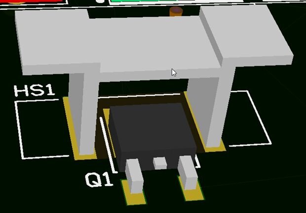
I am using a DPAK power component and an SMD heatsink intended for use with a DPAK device (i.e. DigiKey: HS407-ND). I am curious what the best practice is for creating a schematic symbol and PCB footprint for this? Should the heat sink symbol / footprint simply be part of the electrical component, or it's own component? I would prefer the heatsink to appear as a separate item on the BOM, to make sure that it isn't missed in the procurement process.

  • Cancel

Top Replies

  • e14softwareuk
    e14softwareuk over 7 years ago +1 suggested
    Keeping the device and heatsink as separate components would make sense, they are separate items and this way they would both appear as separate BOM entries. Also gives you more flexibility in future to…
  • r.gibson
    r.gibson over 7 years ago in reply to e14softwareuk +1
    Ok, but how do I handle PCB components that are stacked vertically and share an electrically hot pad, separated only by soldermask?
  • e14softwareuk
    e14softwareuk over 7 years ago in reply to r.gibson +1 suggested
    Would it work to define the heatsink as a dumb item without any active pads/drill holes if it is sharing with the active device?
Parents
  • e14softwareuk
    0 e14softwareuk over 7 years ago

    Keeping the device and heatsink as separate components would make sense, they are separate items and this way they would both appear as separate BOM entries. Also gives you more flexibility in future to upsize/downsize the heatsink if needed for subsequent designs.

    • Cancel
    • Vote Up +1 Vote Down
    • Cancel
Reply
  • e14softwareuk
    0 e14softwareuk over 7 years ago

    Keeping the device and heatsink as separate components would make sense, they are separate items and this way they would both appear as separate BOM entries. Also gives you more flexibility in future to upsize/downsize the heatsink if needed for subsequent designs.

    • Cancel
    • Vote Up +1 Vote Down
    • Cancel
Children
  • r.gibson
    0 r.gibson over 7 years ago in reply to e14softwareuk

    Ok, but how do I handle PCB components that are stacked vertically and share an electrically hot pad, separated only by soldermask?

    • Cancel
    • Vote Up +1 Vote Down
    • Cancel
  • e14softwareuk
    0 e14softwareuk over 7 years ago in reply to r.gibson

    Would it work to define the heatsink as a dumb item without any active pads/drill holes if it is sharing with the active device?

    • Cancel
    • Vote Up +1 Vote Down
    • Cancel
  • r.gibson
    0 r.gibson over 7 years ago in reply to e14softwareuk

    So I think what you're saying is to include the heatsink pads in the electrical component footprint and then define a HS schematic symbol, so it is populated in the BOM and can be located near the associated component graphically for assembly purposes. Then create a blank footprint for the heatsink that only includes reference designator and silkscreen outline? That sounds like it will work. Are there any design rules that will be broken by stacking components like that though?

    • Cancel
    • Vote Up +1 Vote Down
    • Cancel
  • e14softwareuk
    0 e14softwareuk over 7 years ago in reply to r.gibson

    Just tested and it will work without breaking any design rules, I created a HS 3D body that 'floats' higher than the active device and did not receive any violations.


    Another option is to design a combined component of active device and heatsink that will be used for PCB layout. You would then also define a 'mechanical' symbol that is heatsink. This will show on the schematic but not be transferred to the PCB so you will get a heatsink in the BOM. Disadvantage is you don't get an automatic designator appearing on the PCB. If you are using isolating washers for the heatsink then these can be defined as mechanical symbols so that are in the BOM but not on the PCB.

    • Cancel
    • Vote Up +1 Vote Down
    • Cancel
  • r.gibson
    0 r.gibson over 7 years ago in reply to e14softwareuk

    I was also able to successfully create and place them this morning as well. Thank you for your help Peter!

    I ended up adding both a Top Overlay (silk) and Top 3D to the heatsink footprint, while the electrical pads and Top Solder[mask] were added to the DPAK footprint.


    Here is a screenshot of the result:

    image

    • Cancel
    • Vote Up +1 Vote Down
    • Cancel
element14 Community

element14 is the first online community specifically for engineers. Connect with your peers and get expert answers to your questions.

  • Members
  • Learn
  • Technologies
  • Challenges & Projects
  • Products
  • Store
  • About Us
  • Feedback & Support
  • FAQs
  • Terms of Use
  • Privacy Policy
  • Legal and Copyright Notices
  • Sitemap
  • Cookies

An Avnet Company © 2025 Premier Farnell Limited. All Rights Reserved.

Premier Farnell Ltd, registered in England and Wales (no 00876412), registered office: Farnell House, Forge Lane, Leeds LS12 2NE.

ICP 备案号 10220084.

Follow element14

  • X
  • Facebook
  • linkedin
  • YouTube