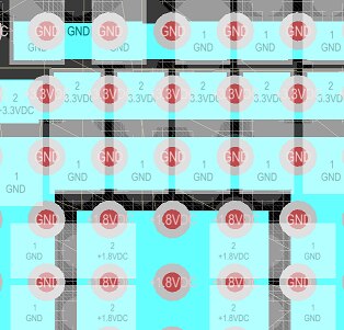
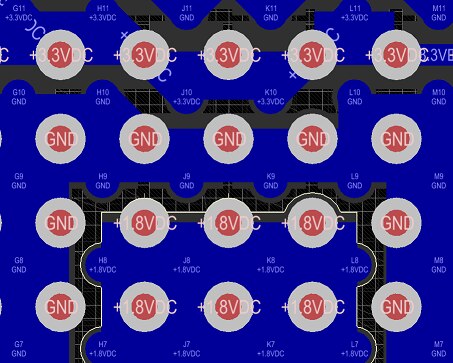
Hello all, yes I'm a noob at PCB design, but I am an experienced Electrical Engineer, so I do have a good handle on electrical theory. I'm currently doing a design that involves an MPU, one DDR2 memory chip and some other items. I have most of the PCB laid out, but now I'm starting to rethink how I did the power/bypass routing for the microprocessor (the first task I did). I've read a lot and looked at designs where they dog-boned all those connections, but I thought it would be more robust if used as thick of tracks as possible and multiple paths for the power to reach the caps and power pins (ONLY for the power, not for signals). However, with reading more about loops, I'm thinking that's not such a good idea and I need to redo it. I'm doing the design on an 8-layer board, so I have 2 ground planes, a 3.3VDC and a 1.8VDC plane with 4 signal layers. I have screen shots of the top and bottom layers here so you can see how I laid them out. I understand the concept of avoiding loops for signal tracks due to signal integrity and noise radiation, but do these same principles apply to power/bypass routing? If my design is wrong, then I would appreciate some advice on proper design and why, I guess I should just individually dog-bone it with the caps between the supply and power pin, if possible. Thanks in advance.
Top layer:
Bottom layer (lighter boxes are caps):