element14 Community
element14 Community
    Register Log In
  • Site
  • Search
  • Log In Register
  • Community Hub
    Community Hub
    • What's New on element14
    • Feedback and Support
    • Benefits of Membership
    • Personal Blogs
    • Members Area
    • Achievement Levels
  • Learn
    Learn
    • Ask an Expert
    • eBooks
    • element14 presents
    • Learning Center
    • Tech Spotlight
    • STEM Academy
    • Webinars, Training and Events
    • Learning Groups
  • Technologies
    Technologies
    • 3D Printing
    • FPGA
    • Industrial Automation
    • Internet of Things
    • Power & Energy
    • Sensors
    • Technology Groups
  • Challenges & Projects
    Challenges & Projects
    • Design Challenges
    • element14 presents Projects
    • Project14
    • Arduino Projects
    • Raspberry Pi Projects
    • Project Groups
  • Products
    Products
    • Arduino
    • Avnet Boards Community
    • Dev Tools
    • Manufacturers
    • Multicomp Pro
    • Product Groups
    • Raspberry Pi
    • RoadTests & Reviews
  • Store
    Store
    • Visit Your Store
    • Choose another store...
      • Europe
      •  Austria (German)
      •  Belgium (Dutch, French)
      •  Bulgaria (Bulgarian)
      •  Czech Republic (Czech)
      •  Denmark (Danish)
      •  Estonia (Estonian)
      •  Finland (Finnish)
      •  France (French)
      •  Germany (German)
      •  Hungary (Hungarian)
      •  Ireland
      •  Israel
      •  Italy (Italian)
      •  Latvia (Latvian)
      •  
      •  Lithuania (Lithuanian)
      •  Netherlands (Dutch)
      •  Norway (Norwegian)
      •  Poland (Polish)
      •  Portugal (Portuguese)
      •  Romania (Romanian)
      •  Russia (Russian)
      •  Slovakia (Slovak)
      •  Slovenia (Slovenian)
      •  Spain (Spanish)
      •  Sweden (Swedish)
      •  Switzerland(German, French)
      •  Turkey (Turkish)
      •  United Kingdom
      • Asia Pacific
      •  Australia
      •  China
      •  Hong Kong
      •  India
      •  Korea (Korean)
      •  Malaysia
      •  New Zealand
      •  Philippines
      •  Singapore
      •  Taiwan
      •  Thailand (Thai)
      • Americas
      •  Brazil (Portuguese)
      •  Canada
      •  Mexico (Spanish)
      •  United States
      Can't find the country/region you're looking for? Visit our export site or find a local distributor.
  • Translate
  • Profile
  • Settings
Altium CircuitStudio
  • Products
  • Manufacturers
  • Altium CircuitStudio
  • More
  • Cancel
Altium CircuitStudio
Altium CircuitStudio Forum Plane Clearance Issue
  • Blog
  • Forum
  • Documents
  • Events
  • Polls
  • Members
  • Mentions
  • Sub-Groups
  • Tags
  • More
  • Cancel
  • New
Join Altium CircuitStudio to participate - click to join for free!
Actions
  • Share
  • More
  • Cancel
Forum Thread Details
  • State Not Answered
  • Locked Locked
  • Replies 3 replies
  • Subscribers 86 subscribers
  • Views 1385 views
  • Users 0 members are here
Related
This discussion has been locked.
You can no longer post new replies to this discussion. If you have a question you can start a new discussion

Plane Clearance Issue

batuu
batuu over 6 years ago

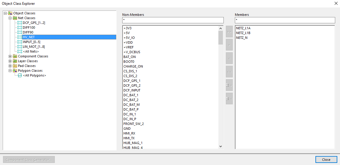
I have a design with high voltage nets. Therefor I have defined a Net Class "HV_NET" with the members NETZ_L1A, NETZ_L1B and NETZ_N.

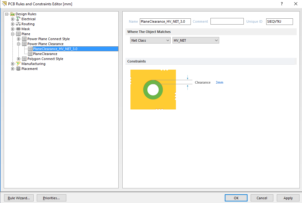
I want to connect the net  "NETZ_L1A" on the Plane 1 layer. The clearance for my HV_NET class should be 3mm, so I created a design rule named "Clearance_HV_NET_3.0" for this.

I also created the power plane clearance rule "Plane_Clearence_HV_NET_3.0".


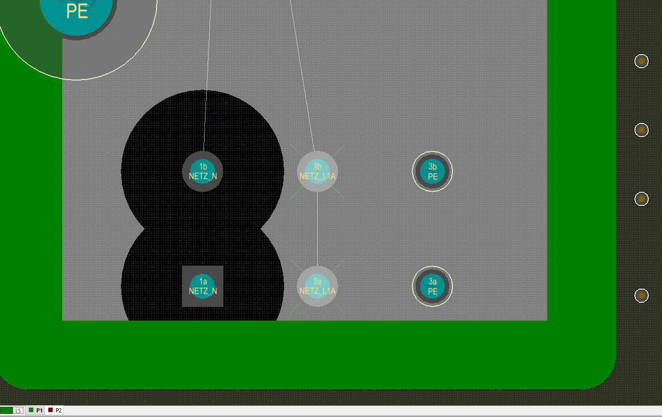
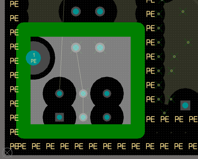
The result is the following. The split plane is assigned to the net "NETZ_L1A". The clearance around the pins with the net NETZ_N are correct. Why there is no clearance around the PE pins and the big PE mounting hole in the upper left.

I get the right result if I assign PE to the HV_NET class, but I do not want to, because then every via like the ones in the right (in the GND split plane area) would get a 3mm clearance.

With my rule set I do not get any design rule check error despite clearance violation between NETZ_L1A and PE.


Any thoughts how to handle this issue? Am I missing something?


Best regards,

Oliver


CS v1.5.2


image


image

image

image

  • Cancel
  • e14softwareuk
    0 e14softwareuk over 6 years ago

    My suggestion would be to set the default plane clearance to 3mm and remove your custom rule. The rule you added means that the place should clear between itself and the new class specified which it has done, all the other clearances use the default rule.

    • Cancel
    • Vote Up 0 Vote Down
    • Cancel
  • batuu
    0 batuu over 6 years ago in reply to e14softwareuk

    Hallo Peter,


    thanks for your suggestion. Sadly this is not what I want.

    With just the default  plane clearance rule set to 3mm I'm getting this:

    image

    I only want the selected area (HV net) within the green box to have a clearance of 3mm to any other net. The split plane outside of the box is GND. I do not want all the PE vias to have a 3mm clearance too.

    Why the electrical clearance rule do not apply for the internal plane layers?


    Oliver

    • Cancel
    • Vote Up 0 Vote Down
    • Cancel
  • e14softwareuk
    0 e14softwareuk over 6 years ago in reply to batuu

    Hi Oliver. I think you will need to switch to drawing your split plane using polygons on a copper layer to be able to configure the design rules needed for this. Create a couple of polygons and name them (e.g. HV, LV), create two polygon classes (one polygon per class) and then add two new Electrical Clearance design rules (one per polygon class). This will give you control over the clearance in each region. To make sure the HV polygon generates the cutout from the larger LV polygon use right click Polygon Actions > Bring To Front so the HV one is processed first.

    • Cancel
    • Vote Up 0 Vote Down
    • Cancel
element14 Community

element14 is the first online community specifically for engineers. Connect with your peers and get expert answers to your questions.

  • Members
  • Learn
  • Technologies
  • Challenges & Projects
  • Products
  • Store
  • About Us
  • Feedback & Support
  • FAQs
  • Terms of Use
  • Privacy Policy
  • Legal and Copyright Notices
  • Sitemap
  • Cookies

An Avnet Company © 2025 Premier Farnell Limited. All Rights Reserved.

Premier Farnell Ltd, registered in England and Wales (no 00876412), registered office: Farnell House, Forge Lane, Leeds LS12 2NE.

ICP 备案号 10220084.

Follow element14

  • X
  • Facebook
  • linkedin
  • YouTube