element14 Community
element14 Community
    Register Log In
  • Site
  • Search
  • Log In Register
  • Community Hub
    Community Hub
    • What's New on element14
    • Feedback and Support
    • Benefits of Membership
    • Personal Blogs
    • Members Area
    • Achievement Levels
  • Learn
    Learn
    • Ask an Expert
    • eBooks
    • element14 presents
    • Learning Center
    • Tech Spotlight
    • STEM Academy
    • Webinars, Training and Events
    • Learning Groups
  • Technologies
    Technologies
    • 3D Printing
    • FPGA
    • Industrial Automation
    • Internet of Things
    • Power & Energy
    • Sensors
    • Technology Groups
  • Challenges & Projects
    Challenges & Projects
    • Design Challenges
    • element14 presents Projects
    • Project14
    • Arduino Projects
    • Raspberry Pi Projects
    • Project Groups
  • Products
    Products
    • Arduino
    • Avnet Boards Community
    • Dev Tools
    • Manufacturers
    • Multicomp Pro
    • Product Groups
    • Raspberry Pi
    • RoadTests & Reviews
  • Store
    Store
    • Visit Your Store
    • Choose another store...
      • Europe
      •  Austria (German)
      •  Belgium (Dutch, French)
      •  Bulgaria (Bulgarian)
      •  Czech Republic (Czech)
      •  Denmark (Danish)
      •  Estonia (Estonian)
      •  Finland (Finnish)
      •  France (French)
      •  Germany (German)
      •  Hungary (Hungarian)
      •  Ireland
      •  Israel
      •  Italy (Italian)
      •  Latvia (Latvian)
      •  
      •  Lithuania (Lithuanian)
      •  Netherlands (Dutch)
      •  Norway (Norwegian)
      •  Poland (Polish)
      •  Portugal (Portuguese)
      •  Romania (Romanian)
      •  Russia (Russian)
      •  Slovakia (Slovak)
      •  Slovenia (Slovenian)
      •  Spain (Spanish)
      •  Sweden (Swedish)
      •  Switzerland(German, French)
      •  Turkey (Turkish)
      •  United Kingdom
      • Asia Pacific
      •  Australia
      •  China
      •  Hong Kong
      •  India
      •  Korea (Korean)
      •  Malaysia
      •  New Zealand
      •  Philippines
      •  Singapore
      •  Taiwan
      •  Thailand (Thai)
      • Americas
      •  Brazil (Portuguese)
      •  Canada
      •  Mexico (Spanish)
      •  United States
      Can't find the country/region you're looking for? Visit our export site or find a local distributor.
  • Translate
  • Profile
  • Settings
Altium CircuitStudio
  • Products
  • Manufacturers
  • Altium CircuitStudio
  • More
  • Cancel
Altium CircuitStudio
Altium CircuitStudio Forum Paste pads disappear
  • Blog
  • Forum
  • Documents
  • Events
  • Polls
  • Members
  • Mentions
  • Sub-Groups
  • Tags
  • More
  • Cancel
  • New
Join Altium CircuitStudio to participate - click to join for free!
Actions
  • Share
  • More
  • Cancel
Forum Thread Details
  • State Not Answered
  • Locked Locked
  • Replies 9 replies
  • Subscribers 87 subscribers
  • Views 1708 views
  • Users 0 members are here
Related
This discussion has been locked.
You can no longer post new replies to this discussion. If you have a question you can start a new discussion

Paste pads disappear

willievisagie
willievisagie over 5 years ago

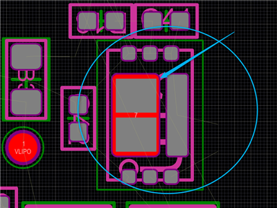
I've had always approached footprints that require complicated paste by setting the paste mask override to some negative number and adding paste pads manually.  However, I found that CircuitStudio (I run version 1.5.2 Build 30) just ignore these paste pads.  When I add the footprint to the PCB the pads are there, but when I save the document, close and reopen CircuitStudio those paste pads are just gone, and the Gerbers generates the same.  So it seems to be a bug in CircuitStudio.  Even if I try to update the footprint, the pads are there, but after save, close and reopen, they're gone.  Has anyone else encountered this?

  • Cancel
  • tarribred61
    0 tarribred61 over 5 years ago

    Hi,


    I have used the same method to modify the paste layers on footprints and have not seen the behavior you report.  For example, I might do this if there is a large exposed pad on a power IC and I want to make the paste stencil into a window pane shape to prevent scoop out of the solder paste. This might appear as below.  The paste layer opening feature is drawn as a fill on top paste and I do not lock it.

    image

    image

    The pad does have a negative value expansion override.


    image


    I have not experienced any problems saving and closing and opening the instantiated part on a PCB design.


    Something to check might be to select the part on the PCB, unlock the primitives and then select the pad that has changed and see if the settings have indeed changed.

    • Cancel
    • Vote Up 0 Vote Down
    • Cancel
  • willievisagie
    0 willievisagie over 5 years ago in reply to tarribred61

    Hi


    Thanks for your reply.  I see that you use fills.  I placed pads on the paste layer.  If you will, please see what happens if you use paste pads instead of paste fills?  Just to confirm the behaviour please?

    • Cancel
    • Vote Up 0 Vote Down
    • Cancel
  • tarribred61
    0 tarribred61 over 5 years ago in reply to tarribred61

    I see you posted the same question in another thread but it is good you made a new one for your problem.  I am also using the same CS version as you report.


    In your post it isn't clear to me exactly what behavior you are seeing.


    Is the pad expansion override not sticking and so the paste layer is appearing the same as the pad or are the added fills on the paste layer disappearing but the pad expansion override is there are you get no paste opening?

    • Cancel
    • Vote Up 0 Vote Down
    • Cancel
  • tarribred61
    0 tarribred61 over 5 years ago in reply to willievisagie

    I'm pretty sure you don't want to put a pad on the paste layer.  Use fills, lines, arcs, circles and such but not pads.


    If you want a complicated shape then I suggest making it using a solid region type object and draw the outline. Then select the properties of the region and change kind property to copper and layer to top paste.

    • Cancel
    • Vote Up 0 Vote Down
    • Cancel
  • willievisagie
    0 willievisagie over 5 years ago in reply to tarribred61

    Hi


    No, that paste override comes through correctly.  CircuitStudio just loses the paste pads after save, close and open.  So at the end, there is no paste at all on the pad.

    • Cancel
    • Vote Up 0 Vote Down
    • Cancel
  • willievisagie
    0 willievisagie over 5 years ago in reply to tarribred61

    It seems like this is the only option.

    I'd like to add that there is no problem at all doing this in Altium Designer.  Never in all the years I've used Altium Designer have I had this problem.  This is the first I see of it in CircuitStudio.

    • Cancel
    • Vote Up 0 Vote Down
    • Cancel
  • tarribred61
    0 tarribred61 over 5 years ago in reply to willievisagie

    I also used AD for about 8 years and Protel SE99 before that and I did not put pads on anything but an outer copper layer.  Pads are by definition a multilayer object.


    Though I would agree it would be better if the software prevented you from putting pads on other layers or at least gave a warning.  Others can correct me if I am wrong.

    • Cancel
    • Vote Up 0 Vote Down
    • Cancel
  • glitch911
    0 glitch911 over 5 years ago

    I noticed same behavior.

    When adding pads only on past layer in my component.

    They disappear after "repour all" operation.

    Then I open the component .pcblib -> view -> library -> right click on component name -> update PCB and get back my custom thermal pad design.

    But I have to be very careful before sending gerber to manufacturer so in my point of view this is a bug that should be fixed.

    • Cancel
    • Vote Up 0 Vote Down
    • Cancel
  • glitch911
    0 glitch911 over 5 years ago in reply to tarribred61

    I agree that is is probably better way to do this but sad thing is that we can't do nice rounded corner this way ;(

    • Cancel
    • Vote Up 0 Vote Down
    • Cancel
element14 Community

element14 is the first online community specifically for engineers. Connect with your peers and get expert answers to your questions.

  • Members
  • Learn
  • Technologies
  • Challenges & Projects
  • Products
  • Store
  • About Us
  • Feedback & Support
  • FAQs
  • Terms of Use
  • Privacy Policy
  • Legal and Copyright Notices
  • Sitemap
  • Cookies

An Avnet Company © 2025 Premier Farnell Limited. All Rights Reserved.

Premier Farnell Ltd, registered in England and Wales (no 00876412), registered office: Farnell House, Forge Lane, Leeds LS12 2NE.

ICP 备案号 10220084.

Follow element14

  • X
  • Facebook
  • linkedin
  • YouTube