element14 Community
element14 Community
    Register Log In
  • Site
  • Search
  • Log In Register
  • About Us
  • Community Hub
    Community Hub
    • What's New on element14
    • Feedback and Support
    • Benefits of Membership
    • Personal Blogs
    • Members Area
    • Achievement Levels
  • Learn
    Learn
    • Ask an Expert
    • eBooks
    • element14 presents
    • Learning Center
    • Tech Spotlight
    • STEM Academy
    • Webinars, Training and Events
    • Learning Groups
  • Technologies
    Technologies
    • 3D Printing
    • FPGA
    • Industrial Automation
    • Internet of Things
    • Power & Energy
    • Sensors
    • Technology Groups
  • Challenges & Projects
    Challenges & Projects
    • Design Challenges
    • element14 presents Projects
    • Project14
    • Arduino Projects
    • Raspberry Pi Projects
    • Project Groups
  • Products
    Products
    • Arduino
    • Avnet Boards Community
    • Dev Tools
    • Manufacturers
    • Multicomp Pro
    • Product Groups
    • Raspberry Pi
    • RoadTests & Reviews
  • Store
    Store
    • Visit Your Store
    • Choose another store...
      • Europe
      •  Austria (German)
      •  Belgium (Dutch, French)
      •  Bulgaria (Bulgarian)
      •  Czech Republic (Czech)
      •  Denmark (Danish)
      •  Estonia (Estonian)
      •  Finland (Finnish)
      •  France (French)
      •  Germany (German)
      •  Hungary (Hungarian)
      •  Ireland
      •  Israel
      •  Italy (Italian)
      •  Latvia (Latvian)
      •  
      •  Lithuania (Lithuanian)
      •  Netherlands (Dutch)
      •  Norway (Norwegian)
      •  Poland (Polish)
      •  Portugal (Portuguese)
      •  Romania (Romanian)
      •  Russia (Russian)
      •  Slovakia (Slovak)
      •  Slovenia (Slovenian)
      •  Spain (Spanish)
      •  Sweden (Swedish)
      •  Switzerland(German, French)
      •  Turkey (Turkish)
      •  United Kingdom
      • Asia Pacific
      •  Australia
      •  China
      •  Hong Kong
      •  India
      •  Korea (Korean)
      •  Malaysia
      •  New Zealand
      •  Philippines
      •  Singapore
      •  Taiwan
      •  Thailand (Thai)
      • Americas
      •  Brazil (Portuguese)
      •  Canada
      •  Mexico (Spanish)
      •  United States
      Can't find the country/region you're looking for? Visit our export site or find a local distributor.
  • Translate
  • Profile
  • Settings
Altium CircuitStudio
  • Products
  • Manufacturers
  • Altium CircuitStudio
  • More
  • Cancel
Altium CircuitStudio
Altium CircuitStudio Forum How to create a 3D aperture inside PCB
  • Blog
  • Forum
  • Documents
  • Events
  • Polls
  • Members
  • Mentions
  • Sub-Groups
  • Tags
  • More
  • Cancel
  • New
Join Altium CircuitStudio to participate - click to join for free!
Actions
  • Share
  • More
  • Cancel
Forum Thread Details
  • State Verified Answer
  • Locked Locked
  • Replies 6 replies
  • Answers 3 answers
  • Subscribers 87 subscribers
  • Views 1054 views
  • Users 0 members are here
Related
This discussion has been locked.
You can no longer post new replies to this discussion. If you have a question you can start a new discussion

How to create a 3D aperture inside PCB

marcogivi
marcogivi over 5 years ago

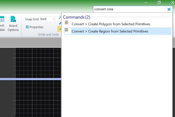
Good morning people!

I need your help. I want create a 3D aperture inside my PCB but I don't konw how.

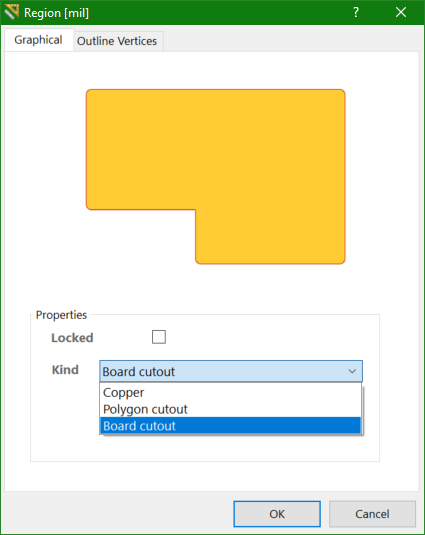
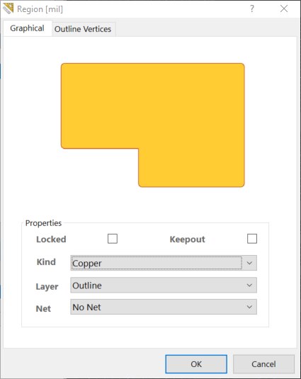
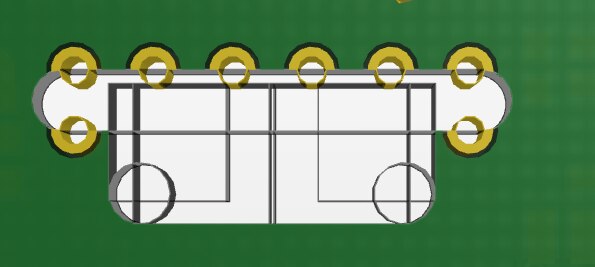
With "Outline layer" I created the shape for my aperture (the shape's not regular...) but now I want create a 3D view where I can see it.

image

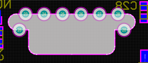
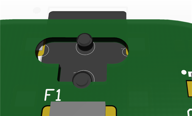
I tried to place a lot of multi-layer pad to create the image but I think it's not correct what I done!

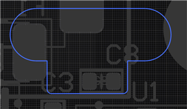
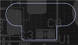
Look the 3D result!!!

image

Please help me.

Have a nice day.

  • Cancel

Top Replies

  • tarribred61
    tarribred61 over 5 years ago +2 suggested
    The tool ribbon has a selection for board cutout that allows you to draw the shape. Also, you can place a solid region on your board outline layer and then select it and make it into a board cutout. You…
  • tarribred61
    tarribred61 over 5 years ago in reply to marcogivi +1 suggested
    Thank you. I should add a few notes and suggestions to finish off this thread. 1) IMPORTANT! Be sure to add a keepout around the cutout region to prevent internal planes and other copper from getting too…
Parents
  • tarribred61
    0 tarribred61 over 5 years ago

    The tool ribbon has a selection for board cutout that allows you to draw the shape.  Also, you can place a solid region on your board outline layer and then select it and make it into a board cutout. 

    image

    You will have to convert your placed objects into the outline of the shape you want.  Possibly do this by tracing the outline or by building the shape on a mechanical layer out of lines and arcs. 

    • Cancel
    • Vote Up +2 Vote Down
    • Cancel
  • marcogivi
    0 marcogivi over 5 years ago in reply to tarribred61

    Thank you Thomas!

    I tried to make what you said me... but I don't understand how to make arcs...

    image

    I drew the outline (pink) and after I drew a region; into the arcs I taked the outline of region and I tried to stay on outline... It's correct?

    Or there's another method?

    • Cancel
    • Vote Up 0 Vote Down
    • Cancel
Reply
  • marcogivi
    0 marcogivi over 5 years ago in reply to tarribred61

    Thank you Thomas!

    I tried to make what you said me... but I don't understand how to make arcs...

    image

    I drew the outline (pink) and after I drew a region; into the arcs I taked the outline of region and I tried to stay on outline... It's correct?

    Or there's another method?

    • Cancel
    • Vote Up 0 Vote Down
    • Cancel
Children
  • tarribred61
    0 tarribred61 over 5 years ago in reply to marcogivi

    Draw your shape on a mechanical layer (for example mech layer 21).

    Place lines and arcs as needed to build the shape. Use a fine line width of 0.05mm or so.

    It looks like you got that far.  If you can select the outline primitives you already made then maybe change them to another mechanical layer.  You don't have to but I think keeping the remnant lines and arcs off on the mechanical layer is better.

    image


    Next, select the primitives you drew.

    image

    Here is the trick....Next go to the search box and start to type convert create... and you should see a command to convert the primitives to a region.

    image

    This should make a region on the mechanical layer. You can move the region around you will still see the old lines and arcs.

    Double click on the region to bring up its properties.

    Change the layer to OUTLINE

    image

    Change the Kind from copper to board cutout.

    Position it where you want it.

    Look in 3D mode.

    image

    • Cancel
    • Vote Up 0 Vote Down
    • Cancel
  • tarribred61
    0 tarribred61 over 5 years ago in reply to tarribred61

    Here is a link to the manpage that describes regions.


    Region | Online Documentation for Altium Products


    It doesn't mention converting primitives to a region but it does show another way to draw arcs to define to outline of the region.  The way they describe may work also but I prefer to work with primitives that I can control dimensions of more easily.

    • Cancel
    • Vote Up 0 Vote Down
    • Cancel
  • marcogivi
    0 marcogivi over 5 years ago in reply to tarribred61

    Thank you very much!

    You are my new IDOL!!!!! image

    I've done it!

    • Cancel
    • Vote Up 0 Vote Down
    • Cancel
  • tarribred61
    0 tarribred61 over 5 years ago in reply to marcogivi

    Thank you.


    I should add a few notes and suggestions to finish off this thread.


    1) IMPORTANT! Be sure to add a keepout around the cutout region to prevent internal planes and other copper from getting too close to the edges of the cutout.

    2) Another benefit of drawing the outline of the cutout region on a mechanical layer is you can add dimension lines and use it to make a mechanical drawing of the board shape.

    3) Simple cutouts can use just holes and/or slots as a non-plated (or plated) feature instead of a region.

    • Cancel
    • Vote Up +1 Vote Down
    • Cancel
element14 Community

element14 is the first online community specifically for engineers. Connect with your peers and get expert answers to your questions.

  • Members
  • Learn
  • Technologies
  • Challenges & Projects
  • Products
  • Store
  • About Us
  • Feedback & Support
  • FAQs
  • Terms of Use
  • Privacy Policy
  • Legal and Copyright Notices
  • Sitemap
  • Cookies

An Avnet Company © 2025 Premier Farnell Limited. All Rights Reserved.

Premier Farnell Ltd, registered in England and Wales (no 00876412), registered office: Farnell House, Forge Lane, Leeds LS12 2NE.

ICP 备案号 10220084.

Follow element14

  • X
  • Facebook
  • linkedin
  • YouTube