element14 Community
element14 Community
    Register Log In
  • Site
  • Search
  • Log In Register
  • Community Hub
    Community Hub
    • What's New on element14
    • Feedback and Support
    • Benefits of Membership
    • Personal Blogs
    • Members Area
    • Achievement Levels
  • Learn
    Learn
    • Ask an Expert
    • eBooks
    • element14 presents
    • Learning Center
    • Tech Spotlight
    • STEM Academy
    • Webinars, Training and Events
    • Learning Groups
  • Technologies
    Technologies
    • 3D Printing
    • FPGA
    • Industrial Automation
    • Internet of Things
    • Power & Energy
    • Sensors
    • Technology Groups
  • Challenges & Projects
    Challenges & Projects
    • Design Challenges
    • element14 presents Projects
    • Project14
    • Arduino Projects
    • Raspberry Pi Projects
    • Project Groups
  • Products
    Products
    • Arduino
    • Avnet & Tria Boards Community
    • Dev Tools
    • Manufacturers
    • Multicomp Pro
    • Product Groups
    • Raspberry Pi
    • RoadTests & Reviews
  • About Us
  • Store
    Store
    • Visit Your Store
    • Choose another store...
      • Europe
      •  Austria (German)
      •  Belgium (Dutch, French)
      •  Bulgaria (Bulgarian)
      •  Czech Republic (Czech)
      •  Denmark (Danish)
      •  Estonia (Estonian)
      •  Finland (Finnish)
      •  France (French)
      •  Germany (German)
      •  Hungary (Hungarian)
      •  Ireland
      •  Israel
      •  Italy (Italian)
      •  Latvia (Latvian)
      •  
      •  Lithuania (Lithuanian)
      •  Netherlands (Dutch)
      •  Norway (Norwegian)
      •  Poland (Polish)
      •  Portugal (Portuguese)
      •  Romania (Romanian)
      •  Russia (Russian)
      •  Slovakia (Slovak)
      •  Slovenia (Slovenian)
      •  Spain (Spanish)
      •  Sweden (Swedish)
      •  Switzerland(German, French)
      •  Turkey (Turkish)
      •  United Kingdom
      • Asia Pacific
      •  Australia
      •  China
      •  Hong Kong
      •  India
      • Japan
      •  Korea (Korean)
      •  Malaysia
      •  New Zealand
      •  Philippines
      •  Singapore
      •  Taiwan
      •  Thailand (Thai)
      • Vietnam
      • Americas
      •  Brazil (Portuguese)
      •  Canada
      •  Mexico (Spanish)
      •  United States
      Can't find the country/region you're looking for? Visit our export site or find a local distributor.
  • Translate
  • Profile
  • Settings
Altium CircuitStudio
  • Products
  • Manufacturers
  • Altium CircuitStudio
  • More
  • Cancel
Altium CircuitStudio
Altium CircuitStudio Forum Clearance difference by layers
  • Blog
  • Forum
  • Documents
  • Events
  • Polls
  • Members
  • Mentions
  • Sub-Groups
  • Tags
  • More
  • Cancel
  • New
Join Altium CircuitStudio to participate - click to join for free!
Actions
  • Share
  • More
  • Cancel
Forum Thread Details
  • State Verified Answer
  • Locked Locked
  • Replies 3 replies
  • Subscribers 89 subscribers
  • Views 881 views
  • Users 0 members are here
  • clearance rule
  • high voltage engineering
  • clearance
  • layer
Related
This discussion has been locked.
You can no longer post new replies to this discussion. If you have a question you can start a new discussion

Clearance difference by layers

ziomau10
ziomau10 over 5 years ago

Hi all,

In some High voltage design it is necessary to impose a large clearance for high voltage nets.

Normally a surface distance have to be considered, like 2.5mm for 250V isolation.

But when the same nets run in some inner layer the distance is not anymore on the surface, but insted in volume.

In volume situation the distance for the same 250V isolation is much less (like .5mm) allowing to pack much more tracks in the same space.
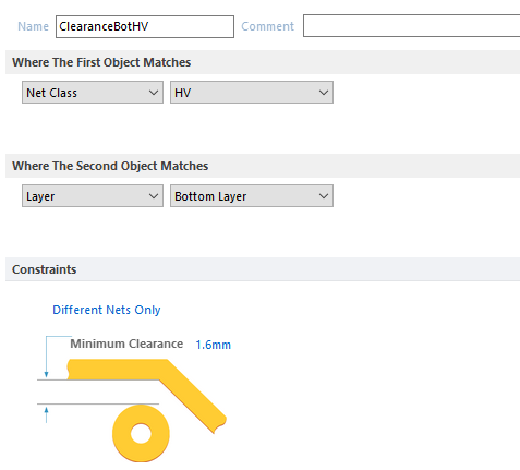
In CS I saw that there is a "Net and Layer" rule that can be used for this purpose, but nothing related to "Net Class".

If on a circuit there are tens or hundredths of nets in the High voltage class I need to type a roule for each net and for each layer.

This may easily add up to thousandths of rules...
Is there a simpler way?


Regards.

Mau.

  • Cancel
  • voltsandjolts
    0 voltsandjolts over 5 years ago

    On a quick test this type of rule seems to set clearance depending on net class and layer:


    image

    • Cancel
    • Vote Up 0 Vote Down
    • Cancel
  • ziomau10
    0 ziomau10 over 5 years ago

    Good!

    I missed that!

    Thank you.

    • Cancel
    • Vote Up 0 Vote Down
    • Cancel
  • voltsandjolts
    0 voltsandjolts over 5 years ago in reply to ziomau10

    If you have a lot of nets in your schematic that need to have a net class applied, it is easier to use a net blanket.

    https://www.eevblog.com/forum/circuit-studio/net-blankets-for-circuitstudio/

    • Cancel
    • Vote Up 0 Vote Down
    • Cancel
element14 Community

element14 is the first online community specifically for engineers. Connect with your peers and get expert answers to your questions.

  • Members
  • Learn
  • Technologies
  • Challenges & Projects
  • Products
  • Store
  • About Us
  • Feedback & Support
  • FAQs
  • Terms of Use
  • Privacy Policy
  • Legal and Copyright Notices
  • Sitemap
  • Cookies

An Avnet Company © 2026 Premier Farnell Limited. All Rights Reserved.

Premier Farnell Ltd, registered in England and Wales (no 00876412), registered office: Farnell House, Forge Lane, Leeds LS12 2NE.

ICP 备案号 10220084.

Follow element14

  • X
  • Facebook
  • linkedin
  • YouTube