element14 Community
element14 Community
    Register Log In
  • Site
  • Search
  • Log In Register
  • About Us
  • Community Hub
    Community Hub
    • What's New on element14
    • Feedback and Support
    • Benefits of Membership
    • Personal Blogs
    • Members Area
    • Achievement Levels
  • Learn
    Learn
    • Ask an Expert
    • eBooks
    • element14 presents
    • Learning Center
    • Tech Spotlight
    • STEM Academy
    • Webinars, Training and Events
    • Learning Groups
  • Technologies
    Technologies
    • 3D Printing
    • FPGA
    • Industrial Automation
    • Internet of Things
    • Power & Energy
    • Sensors
    • Technology Groups
  • Challenges & Projects
    Challenges & Projects
    • Design Challenges
    • element14 presents Projects
    • Project14
    • Arduino Projects
    • Raspberry Pi Projects
    • Project Groups
  • Products
    Products
    • Arduino
    • Avnet Boards Community
    • Dev Tools
    • Manufacturers
    • Multicomp Pro
    • Product Groups
    • Raspberry Pi
    • RoadTests & Reviews
  • Store
    Store
    • Visit Your Store
    • Choose another store...
      • Europe
      •  Austria (German)
      •  Belgium (Dutch, French)
      •  Bulgaria (Bulgarian)
      •  Czech Republic (Czech)
      •  Denmark (Danish)
      •  Estonia (Estonian)
      •  Finland (Finnish)
      •  France (French)
      •  Germany (German)
      •  Hungary (Hungarian)
      •  Ireland
      •  Israel
      •  Italy (Italian)
      •  Latvia (Latvian)
      •  
      •  Lithuania (Lithuanian)
      •  Netherlands (Dutch)
      •  Norway (Norwegian)
      •  Poland (Polish)
      •  Portugal (Portuguese)
      •  Romania (Romanian)
      •  Russia (Russian)
      •  Slovakia (Slovak)
      •  Slovenia (Slovenian)
      •  Spain (Spanish)
      •  Sweden (Swedish)
      •  Switzerland(German, French)
      •  Turkey (Turkish)
      •  United Kingdom
      • Asia Pacific
      •  Australia
      •  China
      •  Hong Kong
      •  India
      •  Korea (Korean)
      •  Malaysia
      •  New Zealand
      •  Philippines
      •  Singapore
      •  Taiwan
      •  Thailand (Thai)
      • Americas
      •  Brazil (Portuguese)
      •  Canada
      •  Mexico (Spanish)
      •  United States
      Can't find the country/region you're looking for? Visit our export site or find a local distributor.
  • Translate
  • Profile
  • Settings
Altium CircuitStudio
  • Products
  • Manufacturers
  • Altium CircuitStudio
  • More
  • Cancel
Altium CircuitStudio
Altium CircuitStudio Forum Polygon Pour on a power layer.
  • Blog
  • Forum
  • Documents
  • Events
  • Polls
  • Members
  • Mentions
  • Sub-Groups
  • Tags
  • More
  • Cancel
  • New
Join Altium CircuitStudio to participate - click to join for free!
Actions
  • Share
  • More
  • Cancel
Forum Thread Details
  • State Not Answered
  • Locked Locked
  • Replies 7 replies
  • Subscribers 89 subscribers
  • Views 1735 views
  • Users 0 members are here
Related
This discussion has been locked.
You can no longer post new replies to this discussion. If you have a question you can start a new discussion

Polygon Pour on a power layer.

lainscough_dfc
lainscough_dfc over 5 years ago

I have four layer board and on the power layer, I want to create an area for +3V3 and +5V


But I cannot select the Power layer?


I must have done something wrong.


image

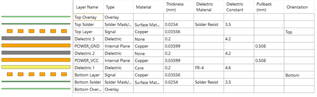
BUT it not allowing me to select the POWER_VCC layer

image


Not sure what I have setup wrong.

Any pointer would be appreciated. Thanks Lee

  • Cancel

Top Replies

  • jeff_electron
    jeff_electron over 5 years ago in reply to lainscough_dfc +1
    long time Altium user here, I have never used actual power plane layers (aka internal planes). a signal layer with a polygon pour on it does everything you need, and has the benefit that its treated like…
  • lainscough_dfc
    0 lainscough_dfc over 5 years ago

    Oh, If I define it as an internal Signal layer it seem to let me do it. I assume Internal planes are treated as negative whole copper plane. OK I might be onto somwthing here. Will investigate once I get back onto it next.

    Comments welcome?

    • Cancel
    • Vote Up 0 Vote Down
    • Cancel
  • tyro01
    0 tyro01 over 5 years ago in reply to lainscough_dfc

    Does this article help you?

    Split Plane | Online Documentation for Altium Products

    • Cancel
    • Vote Up 0 Vote Down
    • Cancel
  • lainscough_dfc
    0 lainscough_dfc over 5 years ago in reply to lainscough_dfc

    Thank, My problem is Ive come from useing a few different tool over the years and the terminology is slightly different on each tool, and its a case of re-training my brain in a way that works with this tool.

    This forum is really great.


    I like CS and for the cost its a great 3D tool. I have tried Kicad but it was too buggy for me to use and Altium products give me a migration path forward which is important.


    Plus lots of part are in Altium format.

    Thanks for your comment.

    • Cancel
    • Vote Up 0 Vote Down
    • Cancel
  • tyro01
    0 tyro01 over 5 years ago in reply to lainscough_dfc

    Yes, I think so too. What you can't do with this product, in many cases, you just don't know how to operate it.

    • Cancel
    • Vote Up 0 Vote Down
    • Cancel
  • jeff_electron
    0 jeff_electron over 5 years ago in reply to lainscough_dfc

    long time Altium user here, I have never used actual power plane layers (aka internal planes). a signal layer with a polygon pour on it does everything you need, and has the benefit that its treated like every other layer so there's less user-interface to learn, and in cases where you really need that layer to run a trace on, you can.

    • Cancel
    • Vote Up +1 Vote Down
    • Cancel
  • tarribred61
    0 tarribred61 over 5 years ago in reply to jeff_electron

    I completely agree.  Planes seem to be relics of the long ago past of hand tape and mylar.

    Edit..

    Maybe of interest.  https://www.altium.com/solution/polygon-or-plane-which-is-better


    Without strongly saying it, they provide the benefits of signal layers over planes and mention the historical reason to use a plane.  They were simpler to define for hand drawn PCBs and early CAD systems and generated smaller Gerber files since you only drew feature where you didn't want copper..  Not much of a benefit now-a-days, in my opinion.

    • Cancel
    • Vote Up 0 Vote Down
    • Cancel
  • lainscough_dfc
    0 lainscough_dfc over 5 years ago in reply to jeff_electron

    Thanks, That's gives me confidence Im going the right direction.

    • Cancel
    • Vote Up 0 Vote Down
    • Cancel
element14 Community

element14 is the first online community specifically for engineers. Connect with your peers and get expert answers to your questions.

  • Members
  • Learn
  • Technologies
  • Challenges & Projects
  • Products
  • Store
  • About Us
  • Feedback & Support
  • FAQs
  • Terms of Use
  • Privacy Policy
  • Legal and Copyright Notices
  • Sitemap
  • Cookies

An Avnet Company © 2025 Premier Farnell Limited. All Rights Reserved.

Premier Farnell Ltd, registered in England and Wales (no 00876412), registered office: Farnell House, Forge Lane, Leeds LS12 2NE.

ICP 备案号 10220084.

Follow element14

  • X
  • Facebook
  • linkedin
  • YouTube