element14 Community
element14 Community
    Register Log In
  • Site
  • Search
  • Log In Register
  • Community Hub
    Community Hub
    • What's New on element14
    • Feedback and Support
    • Benefits of Membership
    • Personal Blogs
    • Members Area
    • Achievement Levels
  • Learn
    Learn
    • Ask an Expert
    • eBooks
    • element14 presents
    • Learning Center
    • Tech Spotlight
    • STEM Academy
    • Webinars, Training and Events
    • Learning Groups
  • Technologies
    Technologies
    • 3D Printing
    • FPGA
    • Industrial Automation
    • Internet of Things
    • Power & Energy
    • Sensors
    • Technology Groups
  • Challenges & Projects
    Challenges & Projects
    • Design Challenges
    • element14 presents Projects
    • Project14
    • Arduino Projects
    • Raspberry Pi Projects
    • Project Groups
  • Products
    Products
    • Arduino
    • Avnet & Tria Boards Community
    • Dev Tools
    • Manufacturers
    • Multicomp Pro
    • Product Groups
    • Raspberry Pi
    • RoadTests & Reviews
  • About Us
  • Store
    Store
    • Visit Your Store
    • Choose another store...
      • Europe
      •  Austria (German)
      •  Belgium (Dutch, French)
      •  Bulgaria (Bulgarian)
      •  Czech Republic (Czech)
      •  Denmark (Danish)
      •  Estonia (Estonian)
      •  Finland (Finnish)
      •  France (French)
      •  Germany (German)
      •  Hungary (Hungarian)
      •  Ireland
      •  Israel
      •  Italy (Italian)
      •  Latvia (Latvian)
      •  
      •  Lithuania (Lithuanian)
      •  Netherlands (Dutch)
      •  Norway (Norwegian)
      •  Poland (Polish)
      •  Portugal (Portuguese)
      •  Romania (Romanian)
      •  Russia (Russian)
      •  Slovakia (Slovak)
      •  Slovenia (Slovenian)
      •  Spain (Spanish)
      •  Sweden (Swedish)
      •  Switzerland(German, French)
      •  Turkey (Turkish)
      •  United Kingdom
      • Asia Pacific
      •  Australia
      •  China
      •  Hong Kong
      •  India
      • Japan
      •  Korea (Korean)
      •  Malaysia
      •  New Zealand
      •  Philippines
      •  Singapore
      •  Taiwan
      •  Thailand (Thai)
      • Vietnam
      • Americas
      •  Brazil (Portuguese)
      •  Canada
      •  Mexico (Spanish)
      •  United States
      Can't find the country/region you're looking for? Visit our export site or find a local distributor.
  • Translate
  • Profile
  • Settings
Altium CircuitStudio
  • Products
  • Manufacturers
  • Altium CircuitStudio
  • More
  • Cancel
Altium CircuitStudio
Altium CircuitStudio Forum Exposed thermal pad footprint design
  • Blog
  • Forum
  • Documents
  • Events
  • Polls
  • Members
  • Mentions
  • Sub-Groups
  • Tags
  • More
  • Cancel
  • New
Join Altium CircuitStudio to participate - click to join for free!
Actions
  • Share
  • More
  • Cancel
Forum Thread Details
  • State Suggested Answer
  • Locked Locked
  • Replies 2 replies
  • Answers 1 answer
  • Subscribers 89 subscribers
  • Views 4014 views
  • Users 0 members are here
Related
This discussion has been locked.
You can no longer post new replies to this discussion. If you have a question you can start a new discussion

Exposed thermal pad footprint design

stuartrumley
stuartrumley over 5 years ago

This question is how to build the circuit symbol and footprint for QFN style packages. A typical QFN may have 40 peripheral pins and one large thermal pad.  A 40 pin QFN, for example, has a 6x6mm package and a thermal pad that is 4.3x4.3mm.  For this size pad I would place an array of 36 10mil vias (0.254mm) all to be connected to ground.  With OrCAD I would explicitly put those 36 ground pad vias in the schematic symbol so that I could ensure they would all be connected to signal ground. that is, the schematic symbol would have 40+36 pins for a total of 76 pins. Then I would use an area for the top layer copper and solder mask.  The solder paste layer is made up an array of uniform rectangles or circles that would occupy about 60% of the copper pad area.  The 60% for the paste seems to be okay for preventing doming and subsequent floating of the chip during reflow.


With Circuit Studio I tried using a large Pad for the thermal pad with an array of vias in the thermal pad.  The Circuit Studio schematic symbol has only one pin in this case for a total of 41 pins.  The problem with is approach is the solder paste aperture will be about the same size as the thermal pad copper and mask.  This is too much solder paste and makes the stencil aperture too large as well (large apertures don't squeegee paste correctly) .


However with CS it looks like I can use one small round pad declared as a through hole via for pin 41 (signal ground) and an additional array of 35 or 36 vias to provide the thermal and RF ground.  The ground pad is now formed as copper area on the top layer with a area defined for the top mask of similar size.  The solder paste is also now an array of small areas grouped symmetrically around the ground pad.


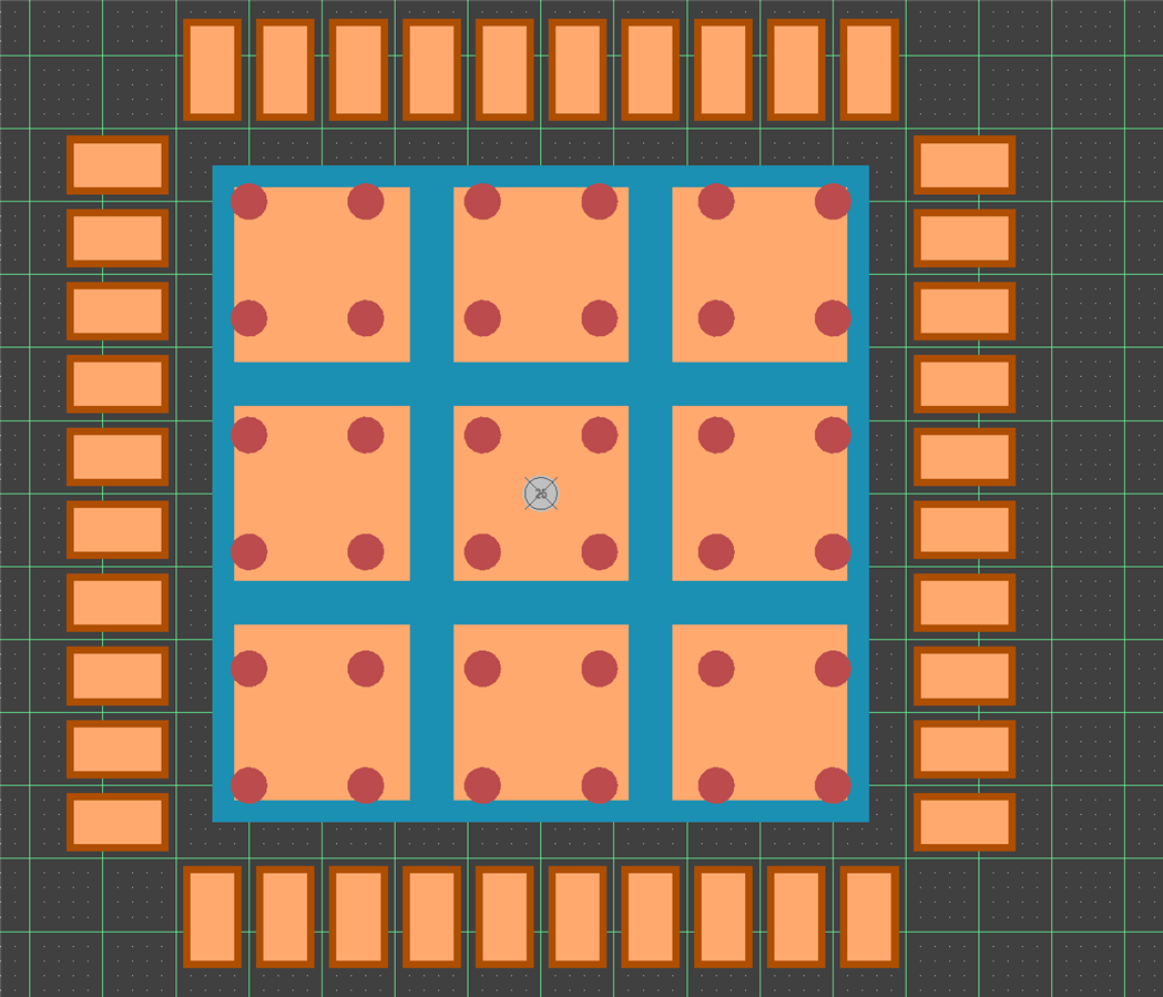
Shown below is the footprint.  This one has 37 ground pad vias with pin 41 in the center of the ground via array.  The solder paste layer is orange, the solder mask is redish, and the copper layer is not shown. This requires a bit of extra work and attention to detail but seems to be the only way to get a correct footprint. tarribred61tarribred61


Here's my question:

1. Will the array of 36 thermal pad vias all get connected to the same net (signal ground) as the center pad (pin 41)?

2. Is there a different or better way to achieve the same result?


image

  • Cancel

Top Replies

  • tarribred61
    tarribred61 over 5 years ago +1 suggested
    Hi Stuart, You seem to have the basic idea of how I do this. For the center pad, I just define an SMT pad without any vias. I adjust the paste mask expansion at the footprint to eliminate the paste mask…
  • tarribred61
    0 tarribred61 over 5 years ago

    Hi Stuart,


    You seem to have the basic idea of how I do this.  For the center pad, I just define an SMT pad without any vias.  I adjust the paste mask expansion at the footprint to eliminate the paste mask entirely.  I leave the solder mask alone so it is defined by rules.


    Then draw what you want on the paste mask layer for openings.


    I prefer to put the vias in at the PCB level so I can define how many and what size they should be there.  Also, I may not need so many if I'm not trying to get the full power and heat out of the part.  If the vias are 10mil or less I don't bother about the solder mask considerations as they are usually too small to thieve away much solder. In fact, my fab notes say that hole tolerance on vias at 10mil (0.25mm) or less can be plated to 0. If the vias are much bigger then you can either fill and plate over or define the solder mask pattern you want similar to how you would define the paste mask.  If you already are using filled and plated via in pads on the board I think it is simpler to just do that.  It can just be a fabrication note callout to fill (with conductive or non-conductive material as you want) and plate.  If it really high volume design and you want to save money then perhaps look into what is best for cost.


    To answer your question #1; The vias in the pad should pick up the net name from the pad net automatically. They do not need their own pins at the schematic level.  If they are in the PCB footprint, you can edit them once they are placed on the PCB but you have to unlock primitives to do that and you should not then update the footprint from the library.  I sometimes have to do this for BGAs with breakouts.  I may not want vias on some of the unused ball pads so as to open up routing channels.


    On question #2; I'm hoping that if someone has a better way they post a reply.

    • Cancel
    • Vote Up +1 Vote Down
    • Cancel
  • stuartrumley
    0 stuartrumley over 5 years ago in reply to tarribred61

    Hi Thomas,

    Okay, I like your idea.  I didn't realize the pad properties would allow me to edit the Paste Mask Expansion sufficiently to eliminate it altogether.  That works much better and from your previous notes, having the vias in the pad will ensure they are netted correctly.

    Thank you so much for your help.

    Stuart

    • Cancel
    • Vote Up 0 Vote Down
    • Cancel
element14 Community

element14 is the first online community specifically for engineers. Connect with your peers and get expert answers to your questions.

  • Members
  • Learn
  • Technologies
  • Challenges & Projects
  • Products
  • Store
  • About Us
  • Feedback & Support
  • FAQs
  • Terms of Use
  • Privacy Policy
  • Legal and Copyright Notices
  • Sitemap
  • Cookies

An Avnet Company © 2026 Premier Farnell Limited. All Rights Reserved.

Premier Farnell Ltd, registered in England and Wales (no 00876412), registered office: Farnell House, Forge Lane, Leeds LS12 2NE.

ICP 备案号 10220084.

Follow element14

  • X
  • Facebook
  • linkedin
  • YouTube